- 您现在的位置:买卖IC网 > PDF目录5369 > ADA4930-2YCPZ-R2 (Analog Devices Inc)IC DIFF AMP 1.35GHZ 24-LFCSP PDF资料下载
参数资料
| 型号: | ADA4930-2YCPZ-R2 |
| 厂商: | Analog Devices Inc |
| 文件页数: | 15/29页 |
| 文件大小: | 0K |
| 描述: | IC DIFF AMP 1.35GHZ 24-LFCSP |
| 标准包装: | 1 |
| 放大器类型: | 差分 |
| 电路数: | 2 |
| 输出类型: | 差分 |
| 转换速率: | 3400 V/µs |
| -3db带宽: | 1.35GHz |
| 电流 - 输入偏压: | 23µA |
| 电压 - 输入偏移: | 150µV |
| 电流 - 电源: | 34mA |
| 电流 - 输出 / 通道: | 30mA |
| 电压 - 电源,单路/双路(±): | 3.3V,5V |
| 工作温度: | -40°C ~ 105°C |
| 安装类型: | 表面贴装 |
| 封装/外壳: | 24-VFQFN 裸露焊盘,CSP |
| 供应商设备封装: | 24-LFCSP-VQ(4x4) |
| 包装: | 标准包装 |
| 其它名称: | ADA4930-2YCPZ-R2DKR |
第1页第2页第3页第4页第5页第6页第7页第8页第9页第10页第11页第12页第13页第14页当前第15页第16页第17页第18页第19页第20页第21页第22页第23页第24页第25页第26页第27页第28页第29页
ADA4930-1/ADA4930-2
Rev. A | Page 21 of 28
Terminating a Single-Ended Input in a Single-Supply
Applications
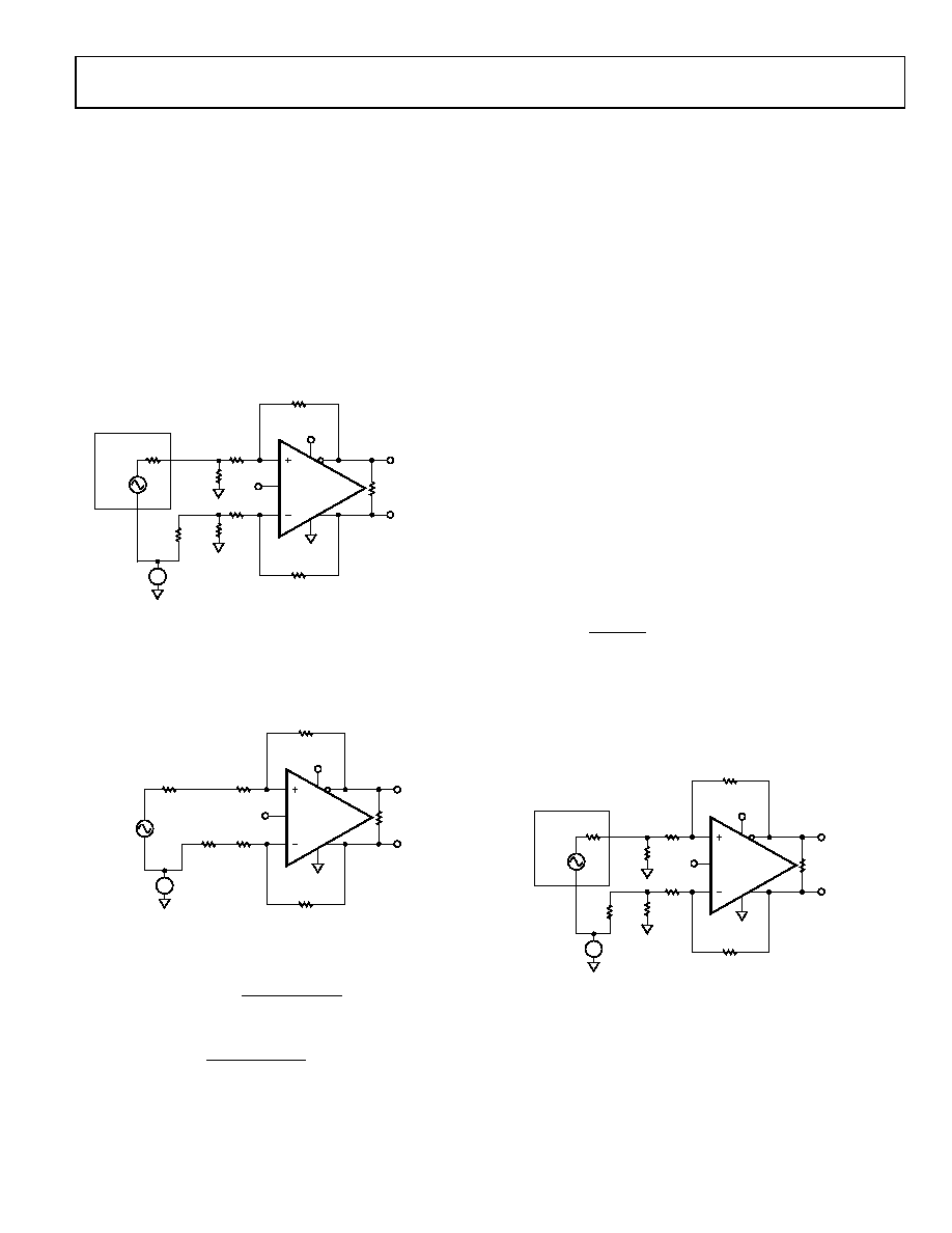
When the application circuit of Figure 50 is powered by a single
supply, the common-mode voltage at the amplifier inputs, VP
and VN, may have to be raised to comply with the specified input
common-mode range. Two methods are available: a dc bias on
the source, as shown in Figure 51, or by connecting resistors RCM
between each input and the supply, as shown on Figure 54.
Input Common-Mode Adjustment with DC Biased Source
To drive a 1.8 V ADC with VCM = 1 V, a 3.3 V single supply
minimizes the power dissipation of the ADA4930-1/ADA4930-2.
The application circuit of Figure 50 on a 3.3 V single supply with a
dc bias added to the source is shown in Figure 51.
ADA4930
RL VOUT, dm
1.990V p-p
3.3V
RS
50
RG1
142
VP
VN
RG2
142
RF2
301
RF1
301
VOCM
VS
2V p-p
VDC
RT
64.2
50
09
20
9-
1
51
Figure 51. Single-Supply, Terminated Single-Ended-to-Differential System with G = 1
To determine the minimum required dc bias, the following steps
must be taken:
1.
Convert the terminated inputs to their Thevenin equivalents,
as shown in the Figure 52 circuit.
ADA4930
RL VOUT, dm
1.99V p-p
3.3V
VON
VOP
RTH
28.11
RG1
142
VP
VN
RG2
142
RF2
301
RF1
301
VOCM
VTH
1.124V p-p
VDC-TH
0
92
09
-15
9
RTH
28.11
Figure 52. Thevenin Equivalent of Single-Supply Application Circuit
2. Write a nodal equation for VP or VN.
()
TH
DC
TH
ON
TH
DC
TH
P
V
+
=
28.11
142
301
OP
TH
DC
N
V
28.11
142
301
+
=
Recognize that while the ADA4930-1/ADA4930-2 is in its
linear operating region, VP and VN are equal. Therefore,
both equations in Step 2 give equal results.
3.
To comply with the minimum specified input common-mode
voltage of 0.3 V at VS = 3.3 V, set the minimum value of VP
and VN to 0.3 V.
4.
Recognize that VP and VN are at their minimum values when
VOP and VS are at their minimum (and therefore VON is at its
maximum).
Let
VP min = VN min = 0.3 V, VOCM = VCM = 1 V, VTH min = VTH/2
VONmax = VOCM + VOUT,dm/4 and VOPmin = VOCM VOUT,dm/4
Substitute conditions into the nodal equation for VP and solve
for VDC-TH.
0.3 = 1.124/2 + VDC-TH + 0.361 × (1 + 1.99/4 = 1.124/2 – VDC-TH)
0.3 + 0.562 0.361 0.18 0.203 = 0.639 VDC-TH
VDC-TH = 0.186 V
Or
Substitute conditions into the nodal equation for VN and
solve for VDC-TH.
0.3 = VDC-TH + 0.361 × (1 1.99/4 VDC-TH)
0.3 – 0.361 + 0.18 = 0.639 × VDC-TH
VDC-TH = 0.186 V
5.
Converting VDC-TH from its Thevenin equivalent results in
V
0.33
0.186
=
×
+
=
TH
S
DC
R
V
The final application circuit is shown in Figure 53. The
additional dc bias of 0.33 V at the inputs ensures that the
minimum input common-mode requirements are met when
the source signal is bipolar with a 2 V p-p amplitude and
VOCM is at 1 V.
3.3V
ADA4930
RL VOUT, dm
1.990V p-p
RS
50
RG1
142
RG2
142
RF2
301
RF1
301
VOCM
VS
2V p-p
RT
64.2
09
20
9-
1
60
VP
VN
50
VDC
0.33V
Figure 53. Single-Supply Application Circuit with DC Source Bias
相关PDF资料 |
PDF描述 |
|---|---|
| 0034.5617.22 | FUSE 1A 250V T-LAG 5X20 SMD T/R |
| KTR10EZPF1804 | RES 1.80M OHM 1/8W 1% 0805 SMD |
| 0034.5619.22 | FUSE 1.6MA 250V TLAG 5X20 SMD TR |
| 0034.5615.22 | FUSE 630MA 250V TLAG 5X20 SMD TR |
| 0034.5609.22 | FUSE 160MA 250V TLAG 5X20 SMD TR |
相关代理商/技术参数 |
参数描述 |
|---|---|
| ADA4930-2YCPZ-R7 | 制造商:Analog Devices 功能描述:SP Amp DIFF AMP Dual 5.5V 24-Pin LFCSP EP T/R 制造商:Analog Devices 功能描述:ULTRALOW NOISE DRIVER FOR LOW VOLT ADC - Tape and Reel 制造商:Analog Devices 功能描述:IC DIFF AMP 1.35GHZ 24-LFCSP 制造商:Analog Devices 功能描述:IC DIFF AMP 1.35GHz 3400V/ us LFCSP- 制造商:Analog Devices 功能描述:IC, DIFF AMP, 1.35GHz, 3400V/ us, LFCSP- 制造商:Analog Devices Inc. 功能描述:Differential Amplifiers UltraLow Noise Driver for Low Volt ADC 制造商:Analog Devices 功能描述:IC, DIFF AMP, 1.35GHz, 3400V/ us, LFCSP-24; No. of Amplifiers:2; Input Offset Voltage:500V; Bandwidth:1.35GHz; Amplifier Case Style:LFCSP; No. of Pins:24; Supply Voltage Range:3.3V to 5V; Slew Rate:3400V/s; Supply Current:34mA ;RoHS Compliant: Yes 制造商:Analog Devices 功能描述:Ultralow Noise Driver for ADCs LFCSP24 |
| ADA4930-2YCPZ-R7_PROMO | 制造商:Analog Devices 功能描述:IC DIFF AMP 1.35GHZ 3400V/U |
| ADA4930-2YCPZ-RL | 功能描述:差分放大器 UltraLow Noise Driver for Low Volt ADC RoHS:否 制造商:Analog Devices 通道数量:1 Channel 带宽:900 MHz 可用增益调整:5.6 dB to 20 dB 输入补偿电压:1 mV at 5 V 共模抑制比(最小值):67 dB 工作电源电压:11 V 电源电流:28 mA 最大工作温度:+ 85 C 最小工作温度:- 40 C 安装风格:SMD/SMT 封装 / 箱体:SOIC-8 封装:Reel |
| ADA4932-1 | 制造商:AD 制造商全称:Analog Devices 功能描述:Low Power Differential ADC Driver |
| ADA4932-1_09 | 制造商:AD 制造商全称:Analog Devices 功能描述:Low Power Differential ADC Driver |
发布紧急采购,3分钟左右您将得到回复。