参数资料
| 型号: | AD8065WARTZ-R7 |
| 厂商: | Analog Devices Inc |
| 文件页数: | 17/29页 |
| 文件大小: | 0K |
| 描述: | IC OPAMP VF R-R LN LP SOT23-5 |
| 标准包装: | 1 |
| 系列: | FastFET™ |
| 放大器类型: | 电压反馈 |
| 电路数: | 1 |
| 输出类型: | 满摆幅 |
| 转换速率: | 180 V/µs |
| -3db带宽: | 145MHz |
| 电流 - 输入偏压: | 3pA |
| 电压 - 输入偏移: | 400µV |
| 电流 - 电源: | 6.6mA |
| 电流 - 输出 / 通道: | 30mA |
| 电压 - 电源,单路/双路(±): | 5 V ~ 24 V |
| 工作温度: | -40°C ~ 105°C |
| 安装类型: | 表面贴装 |
| 封装/外壳: | SC-74A,SOT-753 |
| 供应商设备封装: | SOT-23-5 |
| 包装: | 标准包装 |
| 其它名称: | AD8065WARTZ-R7DKR |
第1页第2页第3页第4页第5页第6页第7页第8页第9页第10页第11页第12页第13页第14页第15页第16页当前第17页第18页第19页第20页第21页第22页第23页第24页第25页第26页第27页第28页第29页
AD8065/AD8066
Rev. J | Page 23 of 28
LAYOUT, GROUNDING, AND BYPASSING CONSIDERATIONS
POWER SUPPLY BYPASSING
Power supply pins are actually inputs and care must be taken so
that a noise-free stable dc voltage is applied. The purpose of bypass
capacitors is to create low impedances from the supply to ground at
all frequencies, thereby shunting or filtering most of the noise.
Decoupling schemes are designed to minimize the bypassing
impedance at all frequencies with a parallel combination of
capacitors. 0.1 μF (X7R or NPO) chip capacitors are critical
and should be as close as possible to the amplifier package.
The 4.7 μF tantalum capacitor is less critical for high frequency
bypassing, and, in most cases, only one is needed per board at
the supply inputs.
GROUNDING
A ground plane layer is important in densely packed PC boards
to spread the current minimizing parasitic inductances. However,
an understanding of where the current flows in a circuit is critical
to implementing effective high speed circuit design. The length
of the current path is directly proportional to the magnitude of
parasitic inductances and, therefore, the high frequency impedance
of the path. High speed currents in an inductive ground return
create unwanted voltage noise.
The length of the high frequency bypass capacitor leads is most
critical. A parasitic inductance in the bypass grounding works
against the low impedance created by the bypass capacitor. Place
the ground leads of the bypass capacitors at the same physical
location. Because load currents flow from the supplies as well,
the ground for the load impedance should be at the same physical
location as the bypass capacitor grounds. For the larger value
capacitors, which are effective at lower frequencies, the current
return path distance is less critical.
LEAKAGE CURRENTS
Poor PC board layout, contaminants, and the board insulator
material can create leakage currents that are much larger than
the input bias current of the AD8065/AD8066. Any voltage
differential between the inputs and nearby runs sets up leakage
currents through the PC board insulator, for example, 1 V/100 GΩ
= 10 pA. Similarly, any contaminants on the board can create
significant leakage (skin oils are a common problem). To reduce
leakage significantly, put a guard ring (shield) around the inputs
and input leads that are driven to the same voltage potential as
the inputs. This way there is no voltage potential between the
inputs and surrounding area to set up any leakage currents.
For the guard ring to be completely effective, it must be driven
by a relatively low impedance source and should completely
surround the input leads on all sides, above and below, using
a multilayer board.
Another effect that can cause leakage currents is the charge
absorption of the insulator material itself. Minimizing the
amount of material between the input leads and the guard ring
helps to reduce the absorption. Also, low absorption materials,
such as Teflon or ceramic, could be necessary in some instances.
INPUT CAPACITANCE
Along with bypassing and ground, high speed amplifiers can be
sensitive to parasitic capacitance between the inputs and ground.
A few pF of capacitance reduces the input impedance at high
frequencies, in turn increasing the amplifier’s gain, causing peaking
of the frequency response or even oscillations, if severe enough.
It is recommended that the external passive components connected
to the input pins be placed as close as possible to the inputs to
avoid parasitic capacitance. The ground and power planes must
be kept at a small distance from the input pins on all layers of
the board.
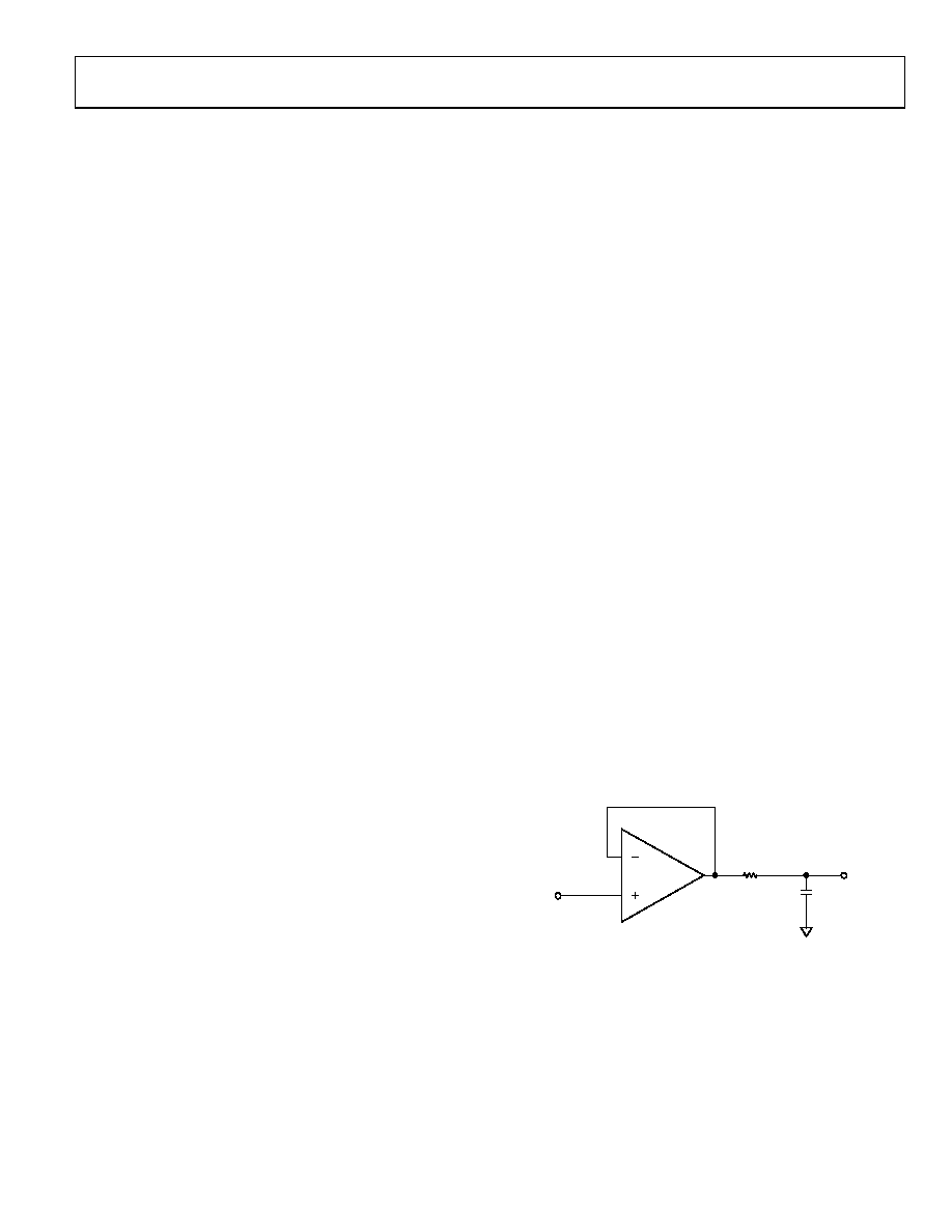
OUTPUT CAPACITANCE
To a lesser extent, parasitic capacitances on the output can cause
peaking and ringing of the frequency response. There are two
methods to effectively minimize their effect:
series with the output to isolate the load capacitor from the
amp’s output stage. A good value to choose is 20 Ω (see
Increase the phase margin with higher noise gains or add
a pole with a parallel resistor and capacitor from IN to
the output.
RS = 20Ω
VI
AD8065
CL
VO
02916-E
-057
Figure 57. Output Isolation Resistor
相关PDF资料 |
PDF描述 |
|---|---|
| PPTC391LGBN | CONN FEMALE 39POS .100" R/A TIN |
| AD8226BRZ-R7 | IC INSTR AMP RRO +/-18 8SOIC |
| NPPN042FJFN-RC | CONN RECEPT 2MM DUAL R/A 8POS |
| AD8216WYRZ-RL | IC AMP 65V DIFF BIDIRECT 8SOIC |
| PPPC082LJBN-RC | CONN FEMALE 16POSDL .1" R/A GOLD |
相关代理商/技术参数 |
参数描述 |
|---|---|
| AD8066AR | 功能描述:IC OPAMP VF R-R DUAL LN LP 8SOIC RoHS:否 类别:集成电路 (IC) >> Linear - Amplifiers - Instrumentation 系列:FastFET™ 标准包装:50 系列:- 放大器类型:J-FET 电路数:2 输出类型:- 转换速率:13 V/µs 增益带宽积:3MHz -3db带宽:- 电流 - 输入偏压:65pA 电压 - 输入偏移:3000µV 电流 - 电源:1.4mA 电流 - 输出 / 通道:- 电压 - 电源,单路/双路(±):7 V ~ 36 V,±3.5 V ~ 18 V 工作温度:-40°C ~ 85°C 安装类型:通孔 封装/外壳:8-DIP(0.300",7.62mm) 供应商设备封装:8-PDIP 包装:管件 |
| AD8066AR-EBZ | 功能描述:BOARD EVAL FOR AD8066AR RoHS:是 类别:编程器,开发系统 >> 评估板 - 运算放大器 系列:- 产品培训模块:Lead (SnPb) Finish for COTS Obsolescence Mitigation Program 标准包装:1 系列:- |
| AD8066ARM | 功能描述:IC OPAMP VF R-R DUAL LN LP 8MSOP RoHS:否 类别:集成电路 (IC) >> Linear - Amplifiers - Instrumentation 系列:FastFET™ 标准包装:50 系列:- 放大器类型:J-FET 电路数:2 输出类型:- 转换速率:13 V/µs 增益带宽积:3MHz -3db带宽:- 电流 - 输入偏压:65pA 电压 - 输入偏移:3000µV 电流 - 电源:1.4mA 电流 - 输出 / 通道:- 电压 - 电源,单路/双路(±):7 V ~ 36 V,±3.5 V ~ 18 V 工作温度:-40°C ~ 85°C 安装类型:通孔 封装/外壳:8-DIP(0.300",7.62mm) 供应商设备封装:8-PDIP 包装:管件 |
| AD8066ARM-EBZ | 功能描述:BOARD EVAL FOR AD8066ARM RoHS:是 类别:编程器,开发系统 >> 评估板 - 运算放大器 系列:- 产品培训模块:Lead (SnPb) Finish for COTS Obsolescence Mitigation Program 标准包装:1 系列:- |
| AD8066ARM-REEL | 制造商:Analog Devices 功能描述:OP Amp Dual Volt Fdbk R-R O/P ±12V/24V 8-Pin MSOP T/R |
发布紧急采购,3分钟左右您将得到回复。