参数资料
| 型号: | AD8142ACPZ-RL |
| 厂商: | Analog Devices Inc |
| 文件页数: | 1/24页 |
| 文件大小: | 0K |
| 描述: | IC VIDEO AMP TRPL DIFF 24LFCSP |
| 标准包装: | 5,000 |
| 应用: | 驱动器 |
| 输出类型: | 差分 |
| 电路数: | 3 |
| -3db带宽: | 285MHz |
| 转换速率: | 1250 V/µs |
| 电流 - 电源: | 47mA |
| 电压 - 电源,单路/双路(±): | 4.5 V ~ 5.5 V,±2.25 V ~ 2.75 V |
| 安装类型: | 表面贴装 |
| 封装/外壳: | 24-WFQFN 裸露焊盘,CSP |
| 供应商设备封装: | 24-LFCSP-WQ(4x4) |
| 包装: | 带卷 (TR) |
Low Cost, Triple Differential Drivers
for Wideband Video
Data Sheet
Rev. A
Information furnished by Analog Devices is believed to be accurate and reliable. However, no
responsibilityisassumedbyAnalogDevicesforitsuse,norforanyinfringementsofpatentsorother
rightsofthirdpartiesthatmayresultfromitsuse.Specificationssubjecttochangewithoutnotice.No
license is granted by implication or otherwise under any patent or patent rights of Analog Devices.
Trademarksandregisteredtrademarksarethepropertyoftheirrespectiveowners.
One Technology Way, P.O. Box 9106, Norwood, MA 02062-9106, U.S.A.
Tel: 781.329.4700
2011–2013 Analog Devices, Inc. All rights reserved.
FEATURES
Triple, high speed differential drivers
255 MHz, 3 dB large signal bandwidth
65 MHz, 0.1 dB flatness
1150 V/s slew rate
12 ns settling time
Single 5 V or split supply operation
Fixed gain of 2
Internal common-mode feedback network
Output balance error 50 dB at 50 MHz
AD8142 has integrated sync-on-common-mode circuitry
High-Z output when disabled
Differential-to-differential or single-ended-to-differential
operation
High isolation between amplifiers: 100 dB at 10 MHz
Low power: 44 mA at 5 V
Available in space-saving packaging: 4 mm × 4 mm LFCSP
APPLICATIONS
Keyboard-video-mouse (KVM) networking
Video distribution
Digital signage
Security cameras
GENERAL DESCRIPTION
The AD8141 and AD8142 are triple, low cost, differential or
single-ended-input-to-differential-output drivers. Each amplifier
has a fixed gain of 2 to compensate for the attenuation of the
line termination resistors. The AD8141 and AD8142 are
specifically designed for RGB signals but can be used for any
type of signals. The amplifiers have very fast slew rate and
settling time while being manufactured on a cost effective
CMOS process. They are optimized for high resolution video
performance with a 0.1 dB flatness of 65 MHz, which allows
driving high resolution video over any type of UTP cable.
The drivers have an internal common-mode feedback loop
that provides output amplitude and phase matching, achieving
50 dB balance error at 50 MHz and thereby suppressing even-
order harmonics and minimizing radiated electromagnetic
interference (EMI).
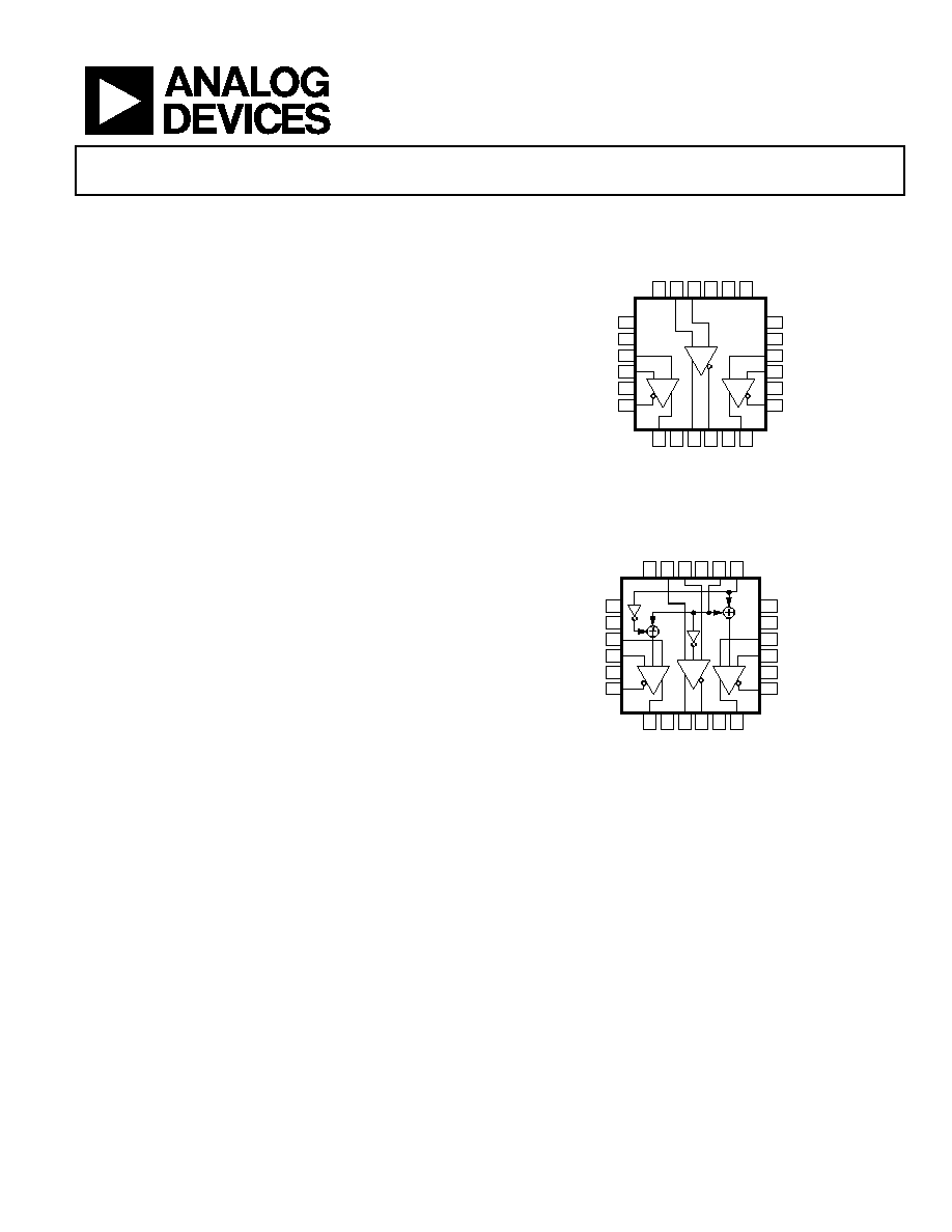
FUNCTIONAL BLOCK DIAGRAMS
09461-
001
1
DIS
2
VS–/GND
3
–IN A
4
+IN A
5
VS–/GND
6
–OUT A
+
OU
T
A
V
S+
+
OU
T
B
–O
UT
B
V
S+
+
OU
T
C
15 +IN C
16 –IN C
17 VS+
18
24 23 22 21 20 19
VOCMC
14 VS–/GND
13
12
11
10
9
8
7
–OUT C
V
S–
/GN
D
+
IN
B
–I
N
B
V
S+
V
O
CM
A
V
O
CM
B
+
–
+
–
+
–
AD8141
Figure 1.
09461-
002
+
OU
T
R
V
S+
+
OU
T
G
–O
UT
G
V
S+
+
OU
T
B
24 23 22 21 20 19
12
11
10
9
8
7
V
S–
/GN
D
+
IN
G
–I
N
G
V
S+
V
SYN
C
H
SYN
C
+
–
+
–
+
–
AD8142
15
16
17
18
14
13
1
2
3
4
5
6
DIS
VS–/GND
–IN R
+IN R
VS–/GND
–OUT R
+IN B
–IN B
VS+
SYNC LEVEL
VS–/GND
–OUT B
×2
Figure 2.
The AD8142 includes a unique sync-on-common-mode feature
that allows the user to transmit balanced horizontal and vertical
video sync signals over the three common-mode channels.
Additionally, the AD8141 and AD8142 both have a disable
feature that, when asserted, produces high-Z outputs, allowing
line isolation and easy multiplexing.
The AD8141 and AD8142 are available in a 24-lead 4 mm × 4 mm
LFCSP and operate over a temperature range of 40°C to +85°C.
They can be used with the AD8145 triple differential-to-single-
line, and the AD8117 or AD8175 crosspoint switches to produce
a high resolution video distribution system.
相关PDF资料 |
PDF描述 |
|---|---|
| VE-B0L-MX-S | CONVERTER MOD DC/DC 28V 75W |
| VI-B3X-MU-F4 | CONVERTER MOD DC/DC 5.2V 200W |
| VE-JTY-MZ-B1 | CONVERTER MOD DC/DC 3.3V 16.5W |
| VE-B0K-MX-S | CONVERTER MOD DC/DC 40V 75W |
| VE-JTX-MZ-B1 | CONVERTER MOD DC/DC 5.2V 25W |
相关代理商/技术参数 |
参数描述 |
|---|---|
| AD8142-EVALZ | 制造商:AD 制造商全称:Analog Devices 功能描述:Low Cost, Triple Differential Drivers |
| AD8143 | 制造商:AD 制造商全称:Analog Devices 功能描述:High Speed, Triple Differential Receiver with Comparators |
| AD8143ACPZ-R2 | 制造商:Analog Devices 功能描述:SP Amp DIFF Receiver Amp Triple 制造商:Analog Devices 功能描述:SP AMP DIFF RCVR AMP TRIPLE 12V/24V 32LFCSP EP - Tape and Reel 制造商:Analog Devices 功能描述:TRIPLE DIFFERENTIAL RECEIVER |
| AD8143ACPZ-REEL | 功能描述:IC RECEIVER TRIPLE DIFF 32LFCSP RoHS:是 类别:集成电路 (IC) >> 接口 - 驱动器,接收器,收发器 系列:- 标准包装:27 系列:- 类型:收发器 驱动器/接收器数:3/3 规程:RS232,RS485 电源电压:4.75 V ~ 5.25 V 安装类型:表面贴装 封装/外壳:28-SOIC(0.295",7.50mm 宽) 供应商设备封装:28-SOIC 包装:管件 |
| AD8143ACPZ-REEL7 | 功能描述:IC RECEIVER TRIPLE DIFF 32LFCSP RoHS:是 类别:集成电路 (IC) >> 接口 - 驱动器,接收器,收发器 系列:- 标准包装:27 系列:- 类型:收发器 驱动器/接收器数:3/3 规程:RS232,RS485 电源电压:4.75 V ~ 5.25 V 安装类型:表面贴装 封装/外壳:28-SOIC(0.295",7.50mm 宽) 供应商设备封装:28-SOIC 包装:管件 |
发布紧急采购,3分钟左右您将得到回复。