参数资料
| 型号: | AD8142ACPZ-RL |
| 厂商: | Analog Devices Inc |
| 文件页数: | 7/24页 |
| 文件大小: | 0K |
| 描述: | IC VIDEO AMP TRPL DIFF 24LFCSP |
| 标准包装: | 5,000 |
| 应用: | 驱动器 |
| 输出类型: | 差分 |
| 电路数: | 3 |
| -3db带宽: | 285MHz |
| 转换速率: | 1250 V/µs |
| 电流 - 电源: | 47mA |
| 电压 - 电源,单路/双路(±): | 4.5 V ~ 5.5 V,±2.25 V ~ 2.75 V |
| 安装类型: | 表面贴装 |
| 封装/外壳: | 24-WFQFN 裸露焊盘,CSP |
| 供应商设备封装: | 24-LFCSP-WQ(4x4) |
| 包装: | 带卷 (TR) |
Data Sheet
AD8141/AD8142
Rev. A | Page 15 of 24
THEORY OF OPERATION
differ from conventional op amps in that they have two outputs
whose voltages move in opposite directions. Like op amps, they
rely on high open-loop gain and negative feedback to force these
drivers make it easy to perform single-ended-to-differential
conversion, common-mode level-shifting, and amplification
of differential signals.
Previous differential drivers, both discrete and integrated designs,
have been based on using two independent amplifiers and two
independent feedback loops, one to control each of the outputs.
When these circuits are driven from a single-ended source, the
resulting outputs are typically not well balanced. Achieving a
balanced output has generally required exceptional matching
of the amplifiers and feedback networks.
DC common-mode level-shifting has also been difficult with
previous differential drivers. Level-shifting has required the
use of a third amplifier and feedback loop to control the output
common-mode level. Sometimes, the third amplifier has also
been used to attempt to correct an inherently unbalanced circuit.
Excellent performance over a wide frequency range has proven
difficult with this approach.
Each AD8141/AD8142 driver uses two feedback loops to
separately control the differential and common-mode output
voltages. The differential feedback, set by the internal resistors,
controls the differential output voltage only. The internal common-
mode feedback loop controls the common-mode output voltage
only. This architecture makes it easy to arbitrarily set the output
common-mode level by simply applying a voltage to the VOCM
input. The output common-mode voltage is forced, by internal
common-mode feedback, to equal the voltage applied to the VOCM
input, while simultaneously balancing the differential output voltage.
The AD8141 VOCM inputs are available to the user, whereas the
AD8142 VOCM inputs are internally connected to sync-on-common-
mode circuitry that automatically imbeds the HSYNC and VSYNC
signals on the three output common-mode voltages.
The overall driver architecture produces outputs that are highly
balanced over a wide frequency range without requiring external
components or adjustments. The common-mode feedback loop
forces the signal component of the output common-mode voltage
to be zeroed. The result is nearly perfectly balanced differential
outputs of identical amplitude that are 180° apart in phase.
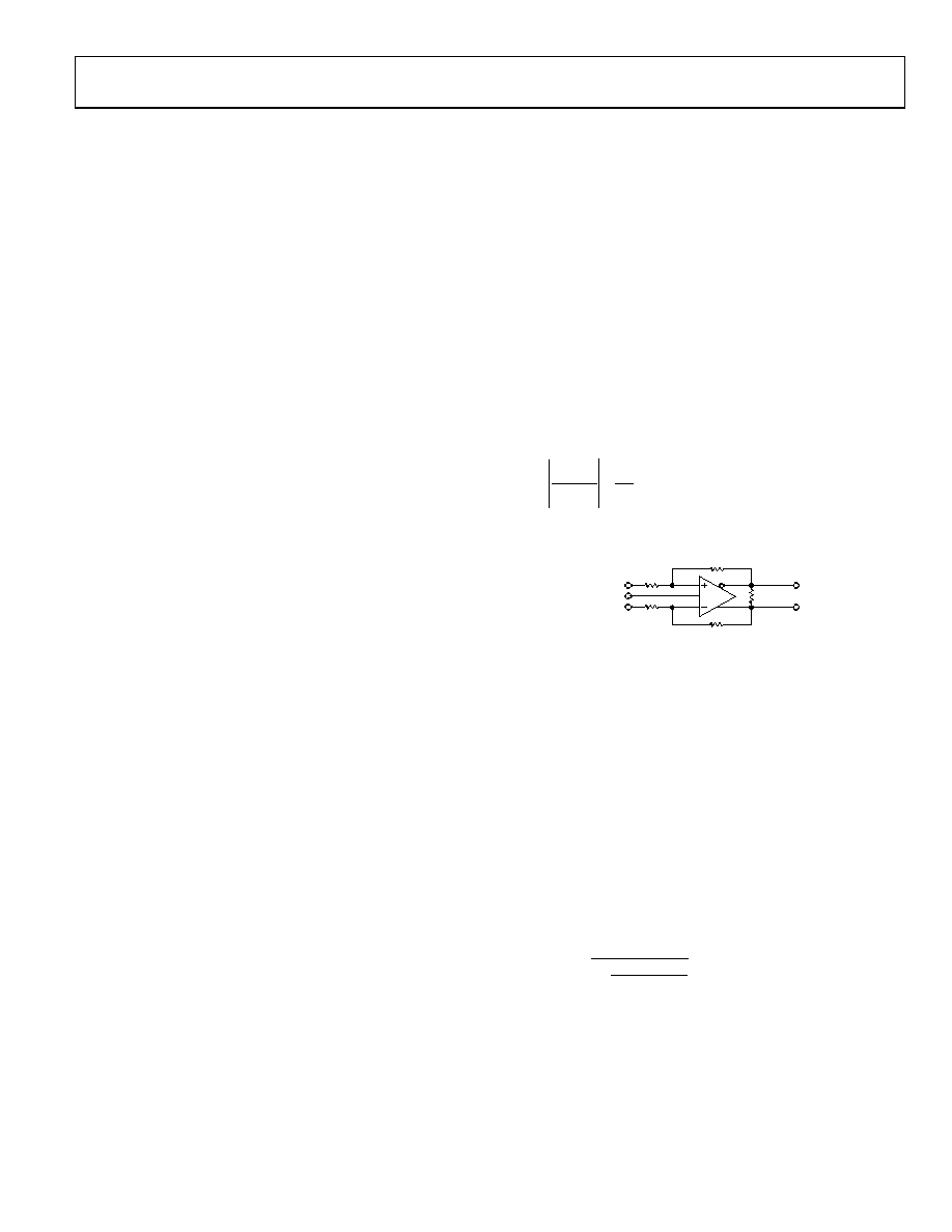
ANALYZING AN APPLICATION CIRCUIT
The drivers use two negative feedback loops, each with high
open-loop gain, to force their differential and common-mode
output voltages in such a way as to minimize the differential
and common-mode input error voltages. The differential input
error voltage is defined as the voltage between the differential
voltage can be assumed to be zero. Similarly, the difference between
the actual output common-mode voltage and the voltage applied to
VOCM can also be assumed to be zero. Starting from these two
assumptions, any application circuit can be analyzed.
CLOSED-LOOP GAIN
The differential mode gain of the circuit in Figure 36 can be
described by
2
=
G
F
dm
IN,
dm
OUT,
R
V
where RF = 2.0 k and RG = 1.0 k nominally.
09461-
034
RF
RG
VAP
VAN
RG
RF
RL, dm
VOUT, dm
VON
VOP
VOCM
VIN, dm
VIP
VIN
+
–
Figure 36. Circuit Definitions
CALCULATING AN APPLICATION CIRCUIT’S INPUT
IMPEDANCE
The effective input impedance of a circuit such as that in Figure 36
at VIP and VIN depends on whether the amplifier is being driven
by a single-ended or differential signal source. For balanced
differential input signals, the differential input impedance, RIN,dm
between the inputs VIP and VIN is simply
RIN, dm = 2 × RG = 2.0 k
In the case of a single-ended input signal (for example, if VIN
is grounded and the input signal is applied to VIP), the input
impedance becomes
(
)
kΩ
5
.
1
2
1
=
+
×
=
F
G
F
G
IN
R
The input impedance of the circuit is higher than for a
conventional op amp connected as an inverter because a
fraction of the differential output voltage appears at the inputs
as a common-mode signal, partially bootstrapping the voltage
across the input resistor RG.
相关PDF资料 |
PDF描述 |
|---|---|
| VE-B0L-MX-S | CONVERTER MOD DC/DC 28V 75W |
| VI-B3X-MU-F4 | CONVERTER MOD DC/DC 5.2V 200W |
| VE-JTY-MZ-B1 | CONVERTER MOD DC/DC 3.3V 16.5W |
| VE-B0K-MX-S | CONVERTER MOD DC/DC 40V 75W |
| VE-JTX-MZ-B1 | CONVERTER MOD DC/DC 5.2V 25W |
相关代理商/技术参数 |
参数描述 |
|---|---|
| AD8142-EVALZ | 制造商:AD 制造商全称:Analog Devices 功能描述:Low Cost, Triple Differential Drivers |
| AD8143 | 制造商:AD 制造商全称:Analog Devices 功能描述:High Speed, Triple Differential Receiver with Comparators |
| AD8143ACPZ-R2 | 制造商:Analog Devices 功能描述:SP Amp DIFF Receiver Amp Triple 制造商:Analog Devices 功能描述:SP AMP DIFF RCVR AMP TRIPLE 12V/24V 32LFCSP EP - Tape and Reel 制造商:Analog Devices 功能描述:TRIPLE DIFFERENTIAL RECEIVER |
| AD8143ACPZ-REEL | 功能描述:IC RECEIVER TRIPLE DIFF 32LFCSP RoHS:是 类别:集成电路 (IC) >> 接口 - 驱动器,接收器,收发器 系列:- 标准包装:27 系列:- 类型:收发器 驱动器/接收器数:3/3 规程:RS232,RS485 电源电压:4.75 V ~ 5.25 V 安装类型:表面贴装 封装/外壳:28-SOIC(0.295",7.50mm 宽) 供应商设备封装:28-SOIC 包装:管件 |
| AD8143ACPZ-REEL7 | 功能描述:IC RECEIVER TRIPLE DIFF 32LFCSP RoHS:是 类别:集成电路 (IC) >> 接口 - 驱动器,接收器,收发器 系列:- 标准包装:27 系列:- 类型:收发器 驱动器/接收器数:3/3 规程:RS232,RS485 电源电压:4.75 V ~ 5.25 V 安装类型:表面贴装 封装/外壳:28-SOIC(0.295",7.50mm 宽) 供应商设备封装:28-SOIC 包装:管件 |
发布紧急采购,3分钟左右您将得到回复。