- 您现在的位置:买卖IC网 > PDF目录11227 > AD8186ARUZ-RL (Analog Devices Inc)IC MULTIPLEXER TRPL 2X1 24TSSOP PDF资料下载
参数资料
| 型号: | AD8186ARUZ-RL |
| 厂商: | Analog Devices Inc |
| 文件页数: | 1/20页 |
| 文件大小: | 0K |
| 描述: | IC MULTIPLEXER TRPL 2X1 24TSSOP |
| 标准包装: | 2,500 |
| 功能: | 多路复用器 |
| 电路: | 3 x 2:1 |
| 电压电源: | 单电源 |
| 电压 - 电源,单路/双路(±): | 3.5 V ~ 5.5 V |
| 工作温度: | -40°C ~ 85°C |
| 安装类型: | 表面贴装 |
| 封装/外壳: | 24-TSSOP(0.173",4.40mm 宽) |
| 供应商设备封装: | 24-TSSOP |
| 包装: | 带卷 (TR) |
REV. A
a
AD8186/AD8187
480 MHz Single-Supply (5 V)
Triple 2:1 Multiplexers
Information furnished by Analog Devices is believed to be accurate and
reliable. However, no responsibility is assumed by Analog Devices for its
use, nor for any infringements of patents or other rights of third parties that
may result from its use. No license is granted by implication or otherwise
under any patent or patent rights of Analog Devices. Trademarks and
registered trademarks are the property of their respective companies.
One Technology Way, P.O. Box 9106, Norwood, MA 02062-9106, U.S.A.
Tel: 781/329-4700
Fax: 781/326-8703
2003 Analog Devices, Inc. All rights reserved.
FEATURES
Fully Buffered Inputs and Outputs
Fast Channel-to-Channel Switching: 4 ns
Single-Supply Operation (5 V)
High Speed:
480 MHz Bandwidth (–3 dB) 2 V p-p
>1600 V/ s (G = +1)
>1500 V/ s (G = +2)
Fast Settling Time of 7 ns to 0.1%
Low Current: 19 mA/20 mA
Excellent Video Specifications (RL = 150
)
0.05% Differential Gain Error
0.05 Differential Phase Error
Low Glitch
All Hostile Crosstalk
–84 dB @ 5 MHz
–52 dB @ 100 MHz
High Off Isolation of –95 dB @ 5 MHz
Low Cost
Fast, High Impedance Disable Feature for Connecting
Multiple Outputs
Logic-Shifted Outputs
APPLICATIONS
Switching RGB in LCD and Plasma Displays
RGB Video Switchers and Routers
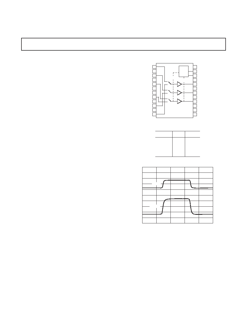
FUNCTIONAL BLOCK DIAGRAM
IN0A
DGND
VREF
OUT 0
OUT 1
OUT 2
IN1A
IN2A
IN2B
IN1B
IN0B
VCC
VEE
VCC
OE
SEL A/
B
VEE
VCC
VEE
DVCC
LOGIC
24
23
22
21
20
19
18
17
16
15
14
13
1
2
3
4
5
6
7
8
9
10
11
12
AD8186/AD8187
0
1
2
SELECT
ENABLE
Table I. Truth Table
SEL A/
B
OE
OUT
00
High Z
10
High Z
11
IN A
01
IN B
GENERAL DESCRIPTION
The AD8186 (G = +1) and AD8187 (G = +2) are high speed,
single-supply, triple 2-to-1 multiplexers. They offer –3 dB large signal
bandwidth of over 480 MHz along with a slew rate in excess of
1500 V/
s. With better than –80 dB of all hostile crosstalk and
–95 dB OFF isolation, they are suited for many high speed appli-
cations. The differential gain and differential phase error of 0.05%
and 0.05
°, along with 0.1 dB flatness to 85 MHz, make the
AD8186 and AD8187 ideal for professional and component video
multiplexing. They offer 4 ns switching time, making them an
excellent choice for switching video signals while consuming less
than 20 mA on a single 5 V supply (100 mW). Both devices have a
high speed disable feature that sets the outputs into a high
impedance state. This allows the building of larger input arrays
while minimizing OFF channel output loading. The devices are
offered in a 24-lead TSSOP package.
TIME (ns)
OUTPUT
V
OL
T
A
GE
(V)
05
10
6.0
5.5
INPUT
V
OL
T
A
GE
(V)
2.5
4.5
4.0
3.5
3.0
2.5
2.0
1.5
1.0
0.5
0
3.0
–0.5
–1.0
3.5
4.0
2.0
1.5
1.0
INPUT
OUTPUT
15
20
5.0
25
Figure 1. AD8187 Video Amplitude Pulse
Response, VOUT = 1.4 V p-p, RL = 150
相关PDF资料 |
PDF描述 |
|---|---|
| AD8187ARUZ-REEL | IC MULTIPLEXER TRPL 2X1 24TSSOP |
| ADG1209YCPZ-REEL | IC MULTIPLEXER DUAL 4X1 16LFCSP |
| VI-J5D-IX-F3 | CONVERTER MOD DC/DC 85V 75W |
| VI-J4X-IX-F2 | CONVERTER MOD DC/DC 5.2V 75W |
| ADG1208YCPZ-REEL | IC MULTIPLEXER 8X1 16LFCSP |
相关代理商/技术参数 |
参数描述 |
|---|---|
| AD8186-EVAL | 制造商:Analog Devices 功能描述:TSSOP TRIPLE 2:1 G=+1 SINGLE SUPPLY MUX - Bulk |
| AD8187 | 制造商:AD 制造商全称:Analog Devices 功能描述:480 MHz Single-Supply (5 V) Triple 2:1 Multiplexers |
| AD8187ARU | 制造商:Analog Devices 功能描述:Analog Multiplexer Triple 2:1 24-Pin TSSOP 制造商:Rochester Electronics LLC 功能描述:TSSOP TRIPLE 2:1 G=+2 SINGLE SUPPLY MUX - Bulk |
| AD8187ARU-REEL | 制造商:Analog Devices 功能描述:Analog Multiplexer Triple 2:1 24-Pin TSSOP T/R |
| AD8187ARU-REEL7 | 制造商:Analog Devices 功能描述:Analog Multiplexer Triple 2:1 24-Pin TSSOP T/R 制造商:Rochester Electronics LLC 功能描述:- Tape and Reel |
发布紧急采购,3分钟左右您将得到回复。