- 您现在的位置:买卖IC网 > PDF目录11227 > AD8186ARUZ-RL (Analog Devices Inc)IC MULTIPLEXER TRPL 2X1 24TSSOP PDF资料下载
参数资料
| 型号: | AD8186ARUZ-RL |
| 厂商: | Analog Devices Inc |
| 文件页数: | 4/20页 |
| 文件大小: | 0K |
| 描述: | IC MULTIPLEXER TRPL 2X1 24TSSOP |
| 标准包装: | 2,500 |
| 功能: | 多路复用器 |
| 电路: | 3 x 2:1 |
| 电压电源: | 单电源 |
| 电压 - 电源,单路/双路(±): | 3.5 V ~ 5.5 V |
| 工作温度: | -40°C ~ 85°C |
| 安装类型: | 表面贴装 |
| 封装/外壳: | 24-TSSOP(0.173",4.40mm 宽) |
| 供应商设备封装: | 24-TSSOP |
| 包装: | 带卷 (TR) |
REV. A
–12–
AD8186/AD8187
THEORY OF OPERATION
The AD8186 (G = +1) and AD8187 (G = +2) are single-supply,
triple 2:1 multiplexers with TTL compatible global input switch-
ing and output-enable control. Optimized for selecting between
two RGB (red, green, blue) video sources, the devices have high
peak slew rates, maintaining their bandwidth for large signals.
Additionally, the multiplexers are compensated for high phase
margin, minimizing overshoot for good pixel resolution. The
multiplexers also have respectable video specifications and are
superior for switching NTSC or PAL composite signals.
The multiplexers are organized as three independent channels,
each with two input transconductance stages and one output
transimpedance stage. The appropriate input transconductance
stages are selected via one logic pin (SEL A/
B) such that all
three outputs switch input connections simultaneously. The
unused input stages are disabled with a proprietary clamp cir-
cuit to provide excellent crosstalk isolation between “on” and
“off ” inputs while protecting the disabled devices from damag-
ing reverse base-emitter voltage stress. No additional input
buffering is necessary, resulting in low input capacitance and
high input impedance without additional signal degradation.
The transconductance stage, a high slew rate, class AB circuit,
sources signal current into a high impedance node. Each output
stage contains a compensation network and is buffered to the
output by a complementary emitter-follower stage. Voltage
feedback sets the gain, with the AD8186 configured as a unity
gain follower and the AD8187 as a gain-of-two amplifier with a
feedback network. This architecture provides drive for a reverse-
terminated video load (150
) with low differential gain and
phase errors while consuming relatively little power. Careful
chip layout and biasing result in excellent crosstalk isolation
between channels.
High Impedance, Output Disable Feature, and Off Isolation
The output-enable logic pin (OE) controls whether the three
outputs are enabled or disabled to a high impedance state.
The high impedance disable allows larger matrices to be built
by busing the outputs together. In the case of the AD8187
(G = +2), a feedback isolation scheme is used so that the
impedance of the gain-of-two feedback network does not load
the output. When not in use, the outputs can be disabled to
reduce power consumption.
The reader may have noticed that the off isolation performance of
the signal path is dependent upon the value of the load resistor,
RL. For calculating off isolation, the signal path may be modeled
as a simple high-pass network with an effective capacitance of
3 fF. Off isolation will improve as the load resistance is decreased. In
the case of the AD8186, off isolation is specified with a 1 k
load. However, a practical application would likely gang the
outputs of multiple muxes. In this case, the proper load resistance
for the off isolation calculation is the output impedance of an
enabled AD8186, typically less than a 10th of an ohm.
Full Power Bandwidth vs. –3 dB Large Signal Bandwidth
Note that full power bandwidth for an undistorted sinusoidal signal
is often calculated using the peak slew rate from the equation
Full Power Bandwidth =
Peak Slew Rate
Sinusoid Amplitude
2
π×
The peak slew rate is not the same as the average slew rate. The
average slew rate is typically specified as the ratio
V
t
OUT
measured between the 20% to 80% output levels of a suffi-
ciently large output pulse. For a natural response, the peak slew
rate may be 2.7 times larger than the average slew rate. There-
fore, calculating a full power bandwidth with a specified average
slew rate will give a pessimistic result. In specifying the large
signal performance of these multiplexers, we’ve published the
large-signal bandwidth, the average slew rate, and the measure-
ments of the total harmonic distortion. (Large signal bandwidth
is defined as the –3 dB point measured on a 2 V p-p output
sine wave.) Specifying these three aspects of the signal path’s
large signal dynamics allows the user to predict system behavior
for either pulse or sinusoid waveforms.
Single-Supply Considerations
DC-Coupled Inputs, Integrated Reference Buffers, and
Selecting the VREF Level on the AD8187, (G = +2)
The AD8186 and AD8187 offer superior large signal dynamics.
The trade-off is that the input and output compliance is limited
to ~1.3 V from either rail when driving a 150
load. These
sections address some challenges of designing video systems
within a single 5 V supply.
The AD8186
The AD8186 is internally wired as a unity-gain follower. Its
inputs and outputs can both swing to within ~1.3 V of either
rail. This affords the user 2.4 V of dynamic range at input and
output, which should be enough for most video signals, whether
the inputs are ac- or dc-coupled. In both cases, the choice of
output termination voltage will determine the quiescent load
current.
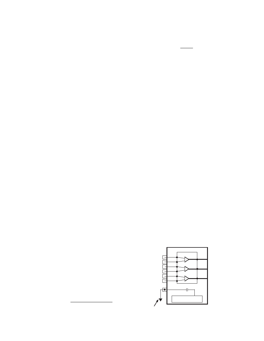
For improved supply rejection, the VREF pin should be tied to
an ac ground (the more quiet supply is a good bet). Internally,
the VREF pin connects to one terminal of an on-chip capacitor.
The capacitor’s other terminal connects to an internal node.
The consequence of building this bypass capacitor on-chip is
twofold. First, the VREF pin on the AD8186 draws no input bias
current. (Contrast this to the case of the AD8187, where the
VREF pin typically draws 2
A of input bias current). Second,
on the AD8186, the VREF pin may be tied to any voltage within
the supply range.
IN0A
IN0B
IN1B
IN1A
IN2A
IN2B
AD8186
OUT0
OUT1
OUT2
MUX SYSTEM
BIAS REFERENCE
INTERNAL CAP
“C_BYPASS”
DIRECT CONNECTION TO ANY “QUIET” AC GROUND
(FOR EXAMPLE, GND, VCC, VEE)
VREF
Figure 3. VREF Pin Connection for AD8186 (Differs
from AD8187)
相关PDF资料 |
PDF描述 |
|---|---|
| AD8187ARUZ-REEL | IC MULTIPLEXER TRPL 2X1 24TSSOP |
| ADG1209YCPZ-REEL | IC MULTIPLEXER DUAL 4X1 16LFCSP |
| VI-J5D-IX-F3 | CONVERTER MOD DC/DC 85V 75W |
| VI-J4X-IX-F2 | CONVERTER MOD DC/DC 5.2V 75W |
| ADG1208YCPZ-REEL | IC MULTIPLEXER 8X1 16LFCSP |
相关代理商/技术参数 |
参数描述 |
|---|---|
| AD8186-EVAL | 制造商:Analog Devices 功能描述:TSSOP TRIPLE 2:1 G=+1 SINGLE SUPPLY MUX - Bulk |
| AD8187 | 制造商:AD 制造商全称:Analog Devices 功能描述:480 MHz Single-Supply (5 V) Triple 2:1 Multiplexers |
| AD8187ARU | 制造商:Analog Devices 功能描述:Analog Multiplexer Triple 2:1 24-Pin TSSOP 制造商:Rochester Electronics LLC 功能描述:TSSOP TRIPLE 2:1 G=+2 SINGLE SUPPLY MUX - Bulk |
| AD8187ARU-REEL | 制造商:Analog Devices 功能描述:Analog Multiplexer Triple 2:1 24-Pin TSSOP T/R |
| AD8187ARU-REEL7 | 制造商:Analog Devices 功能描述:Analog Multiplexer Triple 2:1 24-Pin TSSOP T/R 制造商:Rochester Electronics LLC 功能描述:- Tape and Reel |
发布紧急采购,3分钟左右您将得到回复。