- 您现在的位置:买卖IC网 > PDF目录11213 > AD8191AASTZ-RL (Analog Devices Inc)IC SWITCH HDMI/DVI 4:1 100LQFP PDF资料下载
参数资料
| 型号: | AD8191AASTZ-RL |
| 厂商: | Analog Devices Inc |
| 文件页数: | 10/28页 |
| 文件大小: | 0K |
| 描述: | IC SWITCH HDMI/DVI 4:1 100LQFP |
| 标准包装: | 1,000 |
| 功能: | 开关,DVI/HDMI |
| 电路: | 1 x 16:1 |
| 电压电源: | 单电源 |
| 电压 - 电源,单路/双路(±): | 3 V ~ 3.6 V |
| 工作温度: | -40°C ~ 85°C |
| 安装类型: | 表面贴装 |
| 封装/外壳: | 100-LQFP |
| 供应商设备封装: | 100-LQFP(14x14) |
| 包装: | 带卷 (TR) |
第1页第2页第3页第4页第5页第6页第7页第8页第9页当前第10页第11页第12页第13页第14页第15页第16页第17页第18页第19页第20页第21页第22页第23页第24页第25页第26页第27页第28页
AD8191A
Rev. 0 | Page 18 of 28
SERIAL INTERFACE CONFIGURATION REGISTERS
The serial interface configuration registers can be read and written using the I2C serial control interface, Pin I2C_SDA, and Pin I2C_SCL.
The least significant bits of the AD8191A I2C part address are set by tying Pin I2C_ADDR2, Pin I2C_ADDR1, and Pin I2C_ADDR0 to
3.3 V (Logic 1) or 0 V (Logic 0). As soon as the serial control interface is used, the parallel control interface is disabled until the AD8191A
is reset, as described in the Serial Control Interface section.
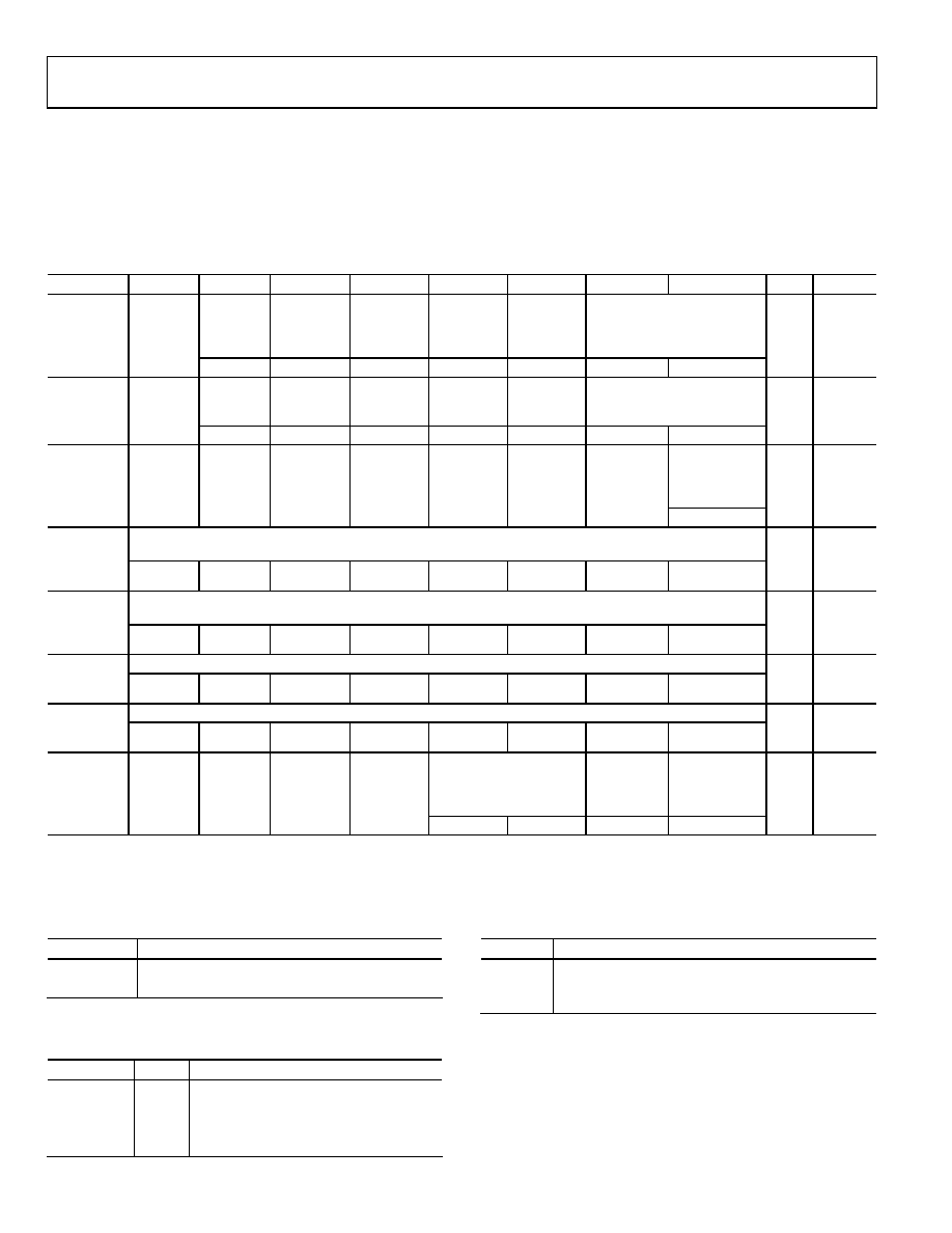
Table 5. Serial (I2C) Interface Register Map
Name
Bit 7
Bit 6
Bit 5
Bit 4
Bit 3
Bit 2
Bit 1
Bit 0
Addr
Default
High
speed
switch
enable
High speed source select
High Speed
Device
Modes
HS_EN
0
HS_CH[1]
HS_CH[0]
0x00
0x40
Auxiliary
switch
enable
Auxiliary switch source select
Auxiliary
Device
Modes
AUX_EN
0
AUX_CH[1]
AUX_CH[0]
0x01
0x40
High speed
input
termination
select
Receiver
Settings
RX_TO
0x10
0x01
Source A and Source B: input termination pulse-on-source switch select
(disconnect termination for a short period of time)
Input
Termination
Pulse
Register 1
RX_PT[7]
RX_PT[6]
RX_PT[5]
RX_PT[4]
RX_PT[3]
RX_PT[2]
RX_PT[1]
RX_PT[0]
0x11
0x00
Source C and Source D: input termination pulse-on-source switch select
(disconnect termination for a short period of time)
Input
Termination
Pulse
Register 2
RX_PT[15]
RX_PO[14]
RX_PT[13]
RX_PT[12]
RX_PT[11]
RX_PT[10]
RX_PT[9]
RX_PT[8]
0x12
0x00
Source A and Source B: input equalization level select
Receive
Equalizer
Register 1
RX_EQ[7]
RX_EQ[6]
RX_EQ[5]
RX_EQ[4]
RX_EQ[3]
RX_EQ[2]
RX_EQ[1]
RX_EQ[0]
0x13
0x00
Source C and Source D: input equalization level select
Receive
Equalizer
Register 2
RX_EQ[15]
RX_EQ[14]
RX_EQ[13]
RX_EQ[12]
RX_EQ[11]
RX_EQ[10]
RX_EQ[9]
RX_EQ[8]
0x14
0x00
High speed output
pre-emphasis level select
High speed
output
termination
select
High speed
output current
level select
Transmitter
Settings
TX_PE[1]
TX_PE[0]
TX_PTO
TX_OCL
0x20
0x03
HIGH SPEED DEVICE MODES REGISTER
HS_EN: High Speed (TMDS) Channels Enable Bit
Table 6. HS_EN Description
HS_EN
Description
0
High speed channels off, low power/standby mode
1
High speed channels on
HS_CH[1:0]: High Speed (TMDS) Switch Source Select Bus
Table 7. HS_CH Mapping
HS_CH[1:0]
O[3:0]
Description
00
A[3:0]
High Speed Source A switched to output
01
B[3:0]
High Speed Source B switched to output
10
C[3:0]
High Speed Source C switched to output
11
D[3:0]
High Speed Source D switched to output
AUXILIARY DEVICE MODES REGISTER
AUX_EN: Auxiliary (Low Speed) Switch Enable Bit
Table 8. AUX_EN Description
AUX_EN
Description
0
Auxiliary switch off, no low speed input/output to
low speed common input/output connection
1
Auxiliary switch on
相关PDF资料 |
PDF描述 |
|---|---|
| AD8191ASTZ-RL | IC INTERFACE HDMI/DVI 100-LQFP |
| VI-B23-IW-F4 | CONVERTER MOD DC/DC 24V 100W |
| VI-B23-IW-F2 | CONVERTER MOD DC/DC 24V 100W |
| VI-B23-IW-F1 | CONVERTER MOD DC/DC 24V 100W |
| VI-B22-IX-F4 | CONVERTER MOD DC/DC 15V 75W |
相关代理商/技术参数 |
参数描述 |
|---|---|
| AD8191AASTZ-RL1 | 制造商:AD 制造商全称:Analog Devices 功能描述:4:1 HDMI/DVI Switch with Equalization |
| AD8191ACPZ | 制造商:Analog Devices 功能描述:- Bulk |
| AD8191A-EVALZ | 制造商:Analog Devices 功能描述:EVAL BD FOR AD8191A - Bulk |
| AD8191A-EVALZ1 | 制造商:AD 制造商全称:Analog Devices 功能描述:4:1 HDMI/DVI Switch with Equalization |
| AD8191ASTZ | 功能描述:IC INTERFACE HDMI/DVI 100-LQFP RoHS:是 类别:集成电路 (IC) >> 接口 - 模拟开关,多路复用器,多路分解器 系列:- 其它有关文件:STG4159 View All Specifications 标准包装:5,000 系列:- 功能:开关 电路:1 x SPDT 导通状态电阻:300 毫欧 电压电源:双电源 电压 - 电源,单路/双路(±):±1.65 V ~ 4.8 V 电流 - 电源:50nA 工作温度:-40°C ~ 85°C 安装类型:表面贴装 封装/外壳:7-WFBGA,FCBGA 供应商设备封装:7-覆晶 包装:带卷 (TR) |
发布紧急采购,3分钟左右您将得到回复。