- 您现在的位置:买卖IC网 > PDF目录11213 > AD8191AASTZ-RL (Analog Devices Inc)IC SWITCH HDMI/DVI 4:1 100LQFP PDF资料下载
参数资料
| 型号: | AD8191AASTZ-RL |
| 厂商: | Analog Devices Inc |
| 文件页数: | 18/28页 |
| 文件大小: | 0K |
| 描述: | IC SWITCH HDMI/DVI 4:1 100LQFP |
| 标准包装: | 1,000 |
| 功能: | 开关,DVI/HDMI |
| 电路: | 1 x 16:1 |
| 电压电源: | 单电源 |
| 电压 - 电源,单路/双路(±): | 3 V ~ 3.6 V |
| 工作温度: | -40°C ~ 85°C |
| 安装类型: | 表面贴装 |
| 封装/外壳: | 100-LQFP |
| 供应商设备封装: | 100-LQFP(14x14) |
| 包装: | 带卷 (TR) |
第1页第2页第3页第4页第5页第6页第7页第8页第9页第10页第11页第12页第13页第14页第15页第16页第17页当前第18页第19页第20页第21页第22页第23页第24页第25页第26页第27页第28页
AD8191A
Rev. 0 | Page 25 of 28
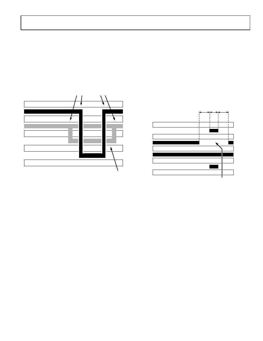
Ground Current Return
In some applications, it can be necessary to invert the output
pin order of the AD8191A, which requires a designer to route
the TMDS traces on multiple layers of the PCB. When routing
differential pairs on multiple layers, it is also necessary to
reroute the corresponding reference plane to provide one
continuous ground current return path for the differential
signals. Standard plated through-hole vias are acceptable for
both the TMDS traces and the reference plane. An example of
this is illustrated in Figure 32.
PCB DIELECTRIC
SILKSCREEN
PCB DIELECTRIC
LAYER 2: GND (REFERENCE PLANE)
LAYER 4: SIGNAL (MICROSTRIP)
THROUGH-HOLE VIAS
LAYER 1: SIGNAL (MICROSTRIP)
KEEP REFERENCE PLANE
ADJACENT TO SIGNAL ON ALL
LAYERS TO PROVIDE CONTINUOUS
GROUND CURRENT RETURN PATH.
LAYER 3: PWR
(REFERENCE PLANE)
07
01
3-
03
5
Figure 32. Example Routing of Reference Plane
Auxiliary Control Signals
There are four single-ended control signals associated with each
source or sink in an HDMI/DVI application: hot plug detect
(HPD), consumer electronics control (CEC), and two display
data channel (DDC) lines. The two signals on the DDC bus are
SDA and SCL (serial data and serial clock, respectively). These
four signals can be switched through the auxiliary bus of the
AD8191A and do not need to be routed with the same strict
considerations as the high speed TMDS signals.
In general, it is sufficient to route each auxiliary signal as a
single-ended trace. These signals are not sensitive to impedance
discontinuities, do not require a reference plane, and can be
routed on multiple layers of the PCB. However, it is best to
follow strict layout practices whenever possible to prevent the
PCB design from affecting the overall application. The specific
routing of the HPD, CEC, and DDC lines depends upon the
application in which the AD8191A is being used.
For example, the maximum speed of signals present on the
auxiliary lines is 100 kHz I2C data on the DDC lines; therefore,
any layout that enables 100 kHz I2C to be passed over the DDC
bus should suffice. The HDMI 1.2a specification, however,
places a strict 50 pF limit on the amount of capacitance that can
be measured on either SDA or SCL at the HDMI input connector.
This 50 pF limit includes the HDMI connector, the PCB, and
whatever capacitance is seen at the input of the AD8191A, or an
equivalent receiver. There is a similar limit of 100 pF of input
capacitance for the CEC line.
The parasitic capacitance of traces on a PCB increases with
trace length. To help ensure that a design satisfies the HDMI
specification, the length of the CEC and DDC lines on the PCB
should be made as short as possible. Additionally, if there is a
reference plane in the layer adjacent to the auxiliary traces in
the PCB stackup, relieving or clearing out this reference plane
directly under the auxiliary traces significantly decreases the
amount of parasitic trace capacitance. An example of the board
stackup is shown in Figure 33.
PCB DIELECTRIC
LAYER 1: SIGNAL (MICROSTRIP)
SILKSCREEN
PCB DIELECTRIC
LAYER 2: GND (REFERENCE PLANE)
LAYER 3: PWR (REFERENCE PLANE)
LAYER 4: SIGNAL (MICROSTRIP)
W
3W
REFERENCE LAYER
RELIEVED UNDERNEATH
MICROSTRIP
07
01
3-
0
32
Figure 33. Example Board Stackup
HPD is a dc signal presented by a sink to a source to indicate
that the source EDID is available for reading. The placement of
this signal is not critical, but it should be routed as directly as
possible.
When the AD8191A is powered up, one set of the auxiliary
inputs is passively routed to the outputs. In this state, the
AD8191A looks like a 100 Ω resistor between the selected
auxiliary inputs and the corresponding outputs, as illustrated in
Figure 27. The AD8191A does not buffer the auxiliary signals;
therefore, the input traces, output traces, and the connection
through the AD8191A all must be considered when designing a
PCB to meet HDMI/DVI specifications. The unselected auxiliary
inputs of the AD8191A are placed into a high impedance mode
when the device is powered up. To ensure that all of the
auxiliary inputs of the AD8191A are in a high impedance mode
when the device is powered off, it is necessary to power the
AMUXVCC supply as illustrated in Figure 28.
In contrast to the auxiliary signals, the AD8191A buffers the
TMDS signals, allowing a PCB designer to layout the TMDS
inputs independently of the outputs.
相关PDF资料 |
PDF描述 |
|---|---|
| AD8191ASTZ-RL | IC INTERFACE HDMI/DVI 100-LQFP |
| VI-B23-IW-F4 | CONVERTER MOD DC/DC 24V 100W |
| VI-B23-IW-F2 | CONVERTER MOD DC/DC 24V 100W |
| VI-B23-IW-F1 | CONVERTER MOD DC/DC 24V 100W |
| VI-B22-IX-F4 | CONVERTER MOD DC/DC 15V 75W |
相关代理商/技术参数 |
参数描述 |
|---|---|
| AD8191AASTZ-RL1 | 制造商:AD 制造商全称:Analog Devices 功能描述:4:1 HDMI/DVI Switch with Equalization |
| AD8191ACPZ | 制造商:Analog Devices 功能描述:- Bulk |
| AD8191A-EVALZ | 制造商:Analog Devices 功能描述:EVAL BD FOR AD8191A - Bulk |
| AD8191A-EVALZ1 | 制造商:AD 制造商全称:Analog Devices 功能描述:4:1 HDMI/DVI Switch with Equalization |
| AD8191ASTZ | 功能描述:IC INTERFACE HDMI/DVI 100-LQFP RoHS:是 类别:集成电路 (IC) >> 接口 - 模拟开关,多路复用器,多路分解器 系列:- 其它有关文件:STG4159 View All Specifications 标准包装:5,000 系列:- 功能:开关 电路:1 x SPDT 导通状态电阻:300 毫欧 电压电源:双电源 电压 - 电源,单路/双路(±):±1.65 V ~ 4.8 V 电流 - 电源:50nA 工作温度:-40°C ~ 85°C 安装类型:表面贴装 封装/外壳:7-WFBGA,FCBGA 供应商设备封装:7-覆晶 包装:带卷 (TR) |
发布紧急采购,3分钟左右您将得到回复。