- 您现在的位置:买卖IC网 > PDF目录11213 > AD8191AASTZ-RL (Analog Devices Inc)IC SWITCH HDMI/DVI 4:1 100LQFP PDF资料下载
参数资料
| 型号: | AD8191AASTZ-RL |
| 厂商: | Analog Devices Inc |
| 文件页数: | 15/28页 |
| 文件大小: | 0K |
| 描述: | IC SWITCH HDMI/DVI 4:1 100LQFP |
| 标准包装: | 1,000 |
| 功能: | 开关,DVI/HDMI |
| 电路: | 1 x 16:1 |
| 电压电源: | 单电源 |
| 电压 - 电源,单路/双路(±): | 3 V ~ 3.6 V |
| 工作温度: | -40°C ~ 85°C |
| 安装类型: | 表面贴装 |
| 封装/外壳: | 100-LQFP |
| 供应商设备封装: | 100-LQFP(14x14) |
| 包装: | 带卷 (TR) |
第1页第2页第3页第4页第5页第6页第7页第8页第9页第10页第11页第12页第13页第14页当前第15页第16页第17页第18页第19页第20页第21页第22页第23页第24页第25页第26页第27页第28页
AD8191A
Rev. 0 | Page 22 of 28
APPLICATIONS INFORMATION
0
70
13
-0
31
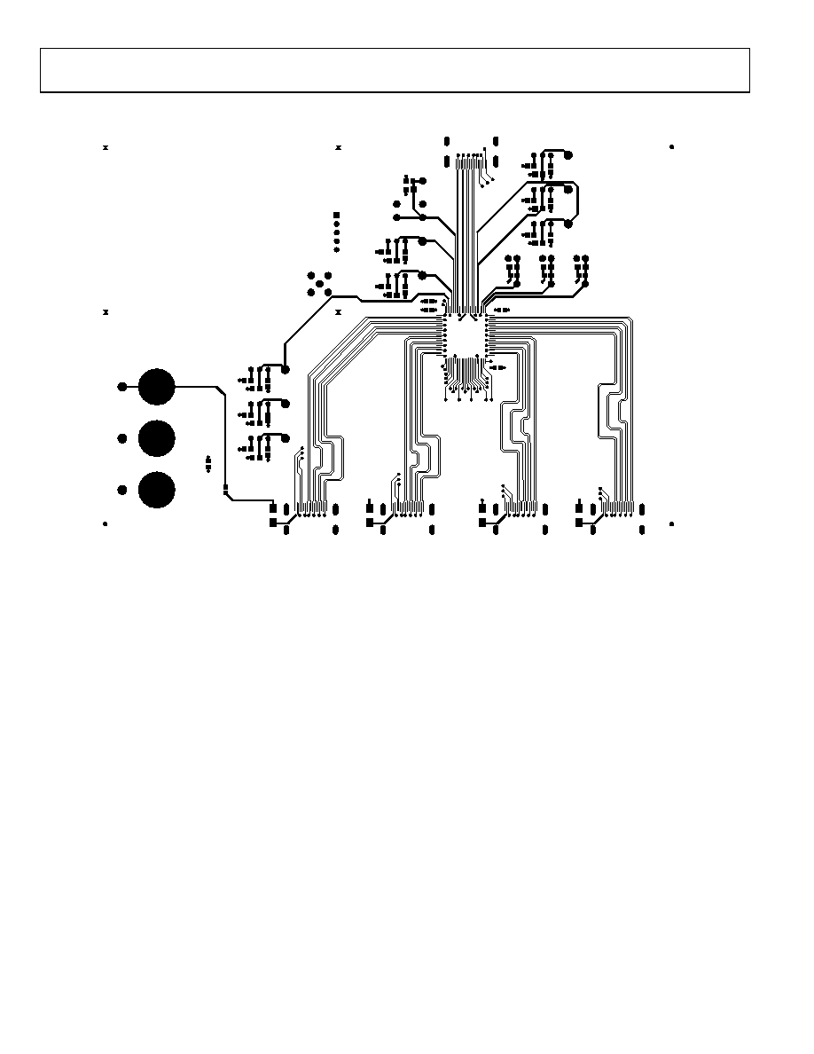
Figure 31. Layout of the TMDS Traces on the AD8191A Evaluation Board (Only Top Signal Routing Layer is Shown)
The AD8191A is an HDMI/DVI switch featuring equalized
TMDS inputs and pre-emphasized TMDS outputs. It is intended
for use as a 4:1 switch in systems with long cable runs on both
the input and/or the output and is fully HDMI 1.2a receive-
compliant.
PINOUT
The AD8191A is designed to have an HDMI/DVI receiver
pinout at its input and a transmitter pinout at its output, which
makes the AD8191A ideal for use in AVR-type applications
where a designer routes both the inputs and the outputs directly
to HDMI/DVI connectors. This type of layout is used on the
AD8191A evaluation board, as shown in Figure 31. When the
AD8191A is used in receiver type applications, it is necessary to
change the order of the output pins on the PCB to align with the
on-board receiver.
One advantage of the AD8191A in an AVR-type application is
that all of the high speed signals can be routed on one side (the
topside) of the board, as shown in Figure 31. In addition to 12 dB of
input equalization, the AD8191A provides up to 6 dB of output
pre-emphasis that boosts the output TMDS signals and allows
the AD8191A to precompensate when driving long
PCB traces or output cables. The net effect of the input
equalization and output pre-emphasis of the AD8191A is that
the AD8191A can compensate for the signal degradation of
both input and output cables; it acts to reopen a closed input
data eye and transmits a full-swing HDMI signal to an end
receiver.
The AD8191A also provides a distinct advantage in receive-type
applications because it is a fully buffered HDMI/DVI switch.
Although inverting the output pin order of the AD8191A on the
PCB requires a designer to place vias in the high speed signal
path, the AD8191A fully buffers and electrically decouples the
outputs from the inputs. Consequently, the effects of the vias
placed on the output signal lines are not seen at the input of the
AD8191A. The programmable output terminations also improve
signal quality at the output of the AD8191A. Therefore, the PCB
designer has significantly improved flexibility in the placement
and routing of the output signal path with the AD8191A over
other solutions.
相关PDF资料 |
PDF描述 |
|---|---|
| AD8191ASTZ-RL | IC INTERFACE HDMI/DVI 100-LQFP |
| VI-B23-IW-F4 | CONVERTER MOD DC/DC 24V 100W |
| VI-B23-IW-F2 | CONVERTER MOD DC/DC 24V 100W |
| VI-B23-IW-F1 | CONVERTER MOD DC/DC 24V 100W |
| VI-B22-IX-F4 | CONVERTER MOD DC/DC 15V 75W |
相关代理商/技术参数 |
参数描述 |
|---|---|
| AD8191AASTZ-RL1 | 制造商:AD 制造商全称:Analog Devices 功能描述:4:1 HDMI/DVI Switch with Equalization |
| AD8191ACPZ | 制造商:Analog Devices 功能描述:- Bulk |
| AD8191A-EVALZ | 制造商:Analog Devices 功能描述:EVAL BD FOR AD8191A - Bulk |
| AD8191A-EVALZ1 | 制造商:AD 制造商全称:Analog Devices 功能描述:4:1 HDMI/DVI Switch with Equalization |
| AD8191ASTZ | 功能描述:IC INTERFACE HDMI/DVI 100-LQFP RoHS:是 类别:集成电路 (IC) >> 接口 - 模拟开关,多路复用器,多路分解器 系列:- 其它有关文件:STG4159 View All Specifications 标准包装:5,000 系列:- 功能:开关 电路:1 x SPDT 导通状态电阻:300 毫欧 电压电源:双电源 电压 - 电源,单路/双路(±):±1.65 V ~ 4.8 V 电流 - 电源:50nA 工作温度:-40°C ~ 85°C 安装类型:表面贴装 封装/外壳:7-WFBGA,FCBGA 供应商设备封装:7-覆晶 包装:带卷 (TR) |
发布紧急采购,3分钟左右您将得到回复。