参数资料
| 型号: | AD823AR |
| 厂商: | Analog Devices Inc |
| 文件页数: | 8/20页 |
| 文件大小: | 0K |
| 描述: | IC OPAMP JFET R-R DUAL LN 8SOIC |
| 标准包装: | 98 |
| 放大器类型: | J-FET |
| 电路数: | 2 |
| 输出类型: | 满摆幅 |
| 转换速率: | 25 V/µs |
| -3db带宽: | 16MHz |
| 电流 - 输入偏压: | 5pA |
| 电压 - 输入偏移: | 700µV |
| 电流 - 电源: | 7mA |
| 电流 - 输出 / 通道: | 17mA |
| 电压 - 电源,单路/双路(±): | 3 V ~ 36 V,±1.5 V ~ 18 V |
| 工作温度: | -40°C ~ 85°C |
| 安装类型: | 表面贴装 |
| 封装/外壳: | 8-SOIC(0.154",3.90mm 宽) |
| 供应商设备封装: | 8-SO |
| 包装: | 管件 |
AD823
Data Sheet
Rev. E | Page 16 of 20
Figure 40 shows a schematic of an AD823 being used to drive
both the input and reference input of an AD1672, a 12-bit,
3-MSPS, single-supply ADC. One amplifier is configured as a
unity-gain follower to drive the analog input of the AD1672,
which is configured to accept an input voltage that ranges from
0 V to 2.5 V.
The other amplifier is configured as a gain of 2 to drive the
reference input from a 1.25 V reference. Although the AD1672
has its own internal reference, there are systems that require
greater accuracy than the internal reference provides. On the other
hand, if the AD1672 internal reference is used, the second AD823
amplifier can be used to buffer the reference voltage for driving
other circuitry while minimally loading the reference source.
13
14
12
11
10
9
8
7
6
5
4
3
2
1
19
18
+5VA
10F
0.1F
2
3
5
6
4
7
1
8
49.9
10F
0.1F
10F
0.1F
+5VA +5VD
+5VD
20
21
22
23
24
25
26
27
16
CLOCK
1k
VIN
VREF
(1.25V)
BIT1 (MSB)
BIT2
BIT3
BIT4
BIT5
BIT6
BIT7
BIT8
BIT9
BIT10
BIT11
BIT12 (LSB)
15
OTR
REFOUT
AIN1
AIN2
REFIN
REFCOM
NCOMP2
NCOMP1
ACOM
CO
M
REF
DCO
M
AD823
+V
CC
+V
DD
28 19
AD1672
00
90
1-
04
0
Figure 40. AD823 Driving Input and Reference of the
AD1672, a 12-Bit, 3-MSPS ADC
The circuit was tested with a 500 kHz sine wave input that was
heavily low-pass filtered (60 dB) to minimize the harmonic content
at the input to the AD823. The digital output of the AD1672 was
analyzed by performing a fast Fourier transform (FFT).
During the testing, it was observed that at 500 kHz, the output
of the AD823 cannot go below ~350 mV (operating with
negative supply at ground) without seriously degrading the
second harmonic distortion. Another test was performed with a
200 Ω pull-down resistor to ground that allowed the output to
go as low as 200 mV without seriously affecting the second
harmonic distortion. There was, however, a slight increase in
the third harmonic term with the resistor added, but it was still
less than the second harmonic.
Figure 41 is an FFT plot of the results of driving the AD1672
with the AD823 with no pull-down resistor. The input
amplitude was 2.15 V p-p and the lower voltage excursion was
350 mV. The input frequency was 490 kHz, which was chosen
to spread the location of the harmonics.
The distortion analysis is important for systems requiring good
frequency domain performance. Other systems may require
good time domain performance. The noise and settling time
performance of the AD823 provides the necessary information
for its applicability for these systems.
5
6
9
3
1
VIN = 2.15V p-p
G = +1
FI = 490kHz
15d
B/
DI
V
7
8
00
90
1-
04
1
2
4
Figure 41. FFT of AD1672 Output Driven by AD823
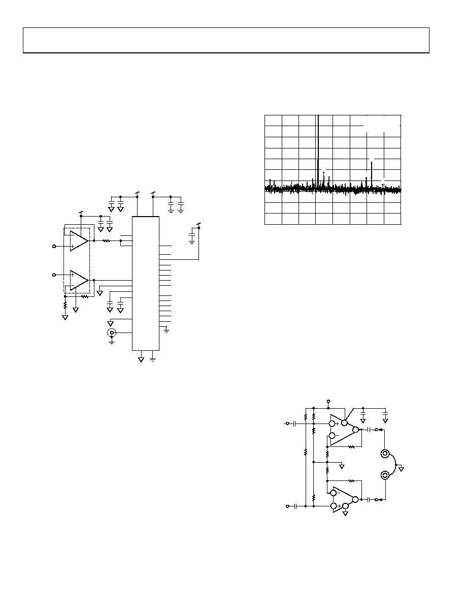
3 V, Single-Supply Stereo Headphone Driver
The AD823 exhibits good current drive and total harmonic
distortion plus noise (THD+N) performance, even at 3 V
single supplies. At 20 kHz, THD+N equals 62 dB (0.079%) for
a 300 mV p-p output signal. This is comparable to other single-
supply op amps that consume more power and cannot run on
3 V power supplies.
In Figure 42, each channel’s input signal is coupled via a 1 μF
Mylar capacitor. Resistor dividers set the dc voltage at the
noninverting inputs so that the output voltage is midway
between the power supplies (+1.5 V). The gain is 1.5. Each half
of the AD823 can then be used to drive a headphone channel. A
5 Hz high-pass filter is realized by the 500 μF capacitors and the
headphones that can be modeled as 32 Ω load resistors to
ground. This ensures that all signals in the audio frequency
range (20 Hz to 20 kHz) are delivered to the headphones.
MYLAR
1F
1/2
AD823
L
R
HEADPHONES
32 IMPEDANCE
4.99k
MYLAR
1F
4.99k
10k
47.5k
95.3k
47.5k
500F
3V
95.3k
0.1F
+
0.1F
CHANNEL 1
CHANNEL 2
95.3k
+
7
4
5
6
1/2
AD823
3
8
2
11
0
090
1-
0
42
Figure 42. 3 V Single-Supply Stereo Headphone Driver
相关PDF资料 |
PDF描述 |
|---|---|
| AD824ARZ-14-3V-RL | IC OPAMP JFET R-R 2MHZ LP 14SOIC |
| AD8250ARMZ-RL | IC AMP INST ICMOS LDRIFT 10MSOP |
| AD8251ARMZ-RL | IC AMP INST ICMOS LDRIFT 10MSOP |
| AD8253ARMZ | IC AMP INST ICMOS LDRIFT 10MSOP |
| AD825AR-REEL7 | IC OPAMP JFET GP 26MHZ 8SOIC |
相关代理商/技术参数 |
参数描述 |
|---|---|
| AD823AR | 制造商:Analog Devices 功能描述:SEMICONDUCTORS LINEAR |
| AD823AR-EBZ | 功能描述:放大器 IC 开发工具 AD823AR-EBZ_A00676_EB-O8R-2Z RoHS:否 制造商:International Rectifier 产品:Demonstration Boards 类型:Power Amplifiers 工具用于评估:IR4302 工作电源电压:13 V to 23 V |
| AD823AR-REEL | 功能描述:IC OPAMP JFET R-R DUAL LN 8SOIC RoHS:否 类别:集成电路 (IC) >> Linear - Amplifiers - Instrumentation 系列:- 标准包装:1 系列:- 放大器类型:通用 电路数:4 输出类型:满摆幅 转换速率:0.028 V/µs 增益带宽积:105kHz -3db带宽:- 电流 - 输入偏压:3nA 电压 - 输入偏移:100µV 电流 - 电源:3.3µA 电流 - 输出 / 通道:12mA 电压 - 电源,单路/双路(±):2.7 V ~ 12 V,±1.35 V ~ 6 V 工作温度:-40°C ~ 85°C 安装类型:表面贴装 封装/外壳:14-TSSOP(0.173",4.40mm 宽) 供应商设备封装:14-TSSOP 包装:剪切带 (CT) 其它名称:OP481GRUZ-REELCT |
| AD823AR-REEL7 | 功能描述:IC OPAMP JFET R-R DUAL LN 8SOIC RoHS:否 类别:集成电路 (IC) >> Linear - Amplifiers - Instrumentation 系列:- 标准包装:73 系列:Over-The-Top® 放大器类型:通用 电路数:4 输出类型:满摆幅 转换速率:0.07 V/µs 增益带宽积:200kHz -3db带宽:- 电流 - 输入偏压:1nA 电压 - 输入偏移:285µV 电流 - 电源:50µA 电流 - 输出 / 通道:25mA 电压 - 电源,单路/双路(±):2 V ~ 44 V,±1 V ~ 22 V 工作温度:-40°C ~ 85°C 安装类型:表面贴装 封装/外壳:16-WFDFN 裸露焊盘 供应商设备封装:16-DFN-EP(5x3) 包装:管件 |
| AD823ARZ | 功能描述:IC OPAMP JFET R-R DUAL LN 8SOIC RoHS:是 类别:集成电路 (IC) >> Linear - Amplifiers - Instrumentation 系列:- 标准包装:2,500 系列:- 放大器类型:通用 电路数:4 输出类型:- 转换速率:0.6 V/µs 增益带宽积:1MHz -3db带宽:- 电流 - 输入偏压:45nA 电压 - 输入偏移:2000µV 电流 - 电源:1.4mA 电流 - 输出 / 通道:40mA 电压 - 电源,单路/双路(±):3 V ~ 32 V,±1.5 V ~ 16 V 工作温度:0°C ~ 70°C 安装类型:表面贴装 封装/外壳:14-TSSOP(0.173",4.40mm 宽) 供应商设备封装:14-TSSOP 包装:带卷 (TR) 其它名称:LM324ADTBR2G-NDLM324ADTBR2GOSTR |
发布紧急采购,3分钟左右您将得到回复。