- 您现在的位置:买卖IC网 > PDF目录5746 > AD824AR-14-REEL (Analog Devices Inc)IC OPAMP JFET R-R 2MHZ LP 14SOIC PDF资料下载
参数资料
| 型号: | AD824AR-14-REEL |
| 厂商: | Analog Devices Inc |
| 文件页数: | 5/16页 |
| 文件大小: | 0K |
| 描述: | IC OPAMP JFET R-R 2MHZ LP 14SOIC |
| 标准包装: | 2,500 |
| 放大器类型: | J-FET |
| 电路数: | 4 |
| 输出类型: | 满摆幅 |
| 转换速率: | 2 V/µs |
| 增益带宽积: | 2MHz |
| -3db带宽: | 2MHz |
| 电流 - 输入偏压: | 4pA |
| 电压 - 输入偏移: | 500µV |
| 电流 - 电源: | 560µA |
| 电流 - 输出 / 通道: | 12mA |
| 电压 - 电源,单路/双路(±): | 3 V ~ 30 V,±1.5 V ~ 15 V |
| 工作温度: | -40°C ~ 85°C |
| 安装类型: | 表面贴装 |
| 封装/外壳: | 14-SOIC(0.154",3.90mm 宽) |
| 供应商设备封装: | 14-SOIC |
| 包装: | 带卷 (TR) |
REV. C
AD824
–13–
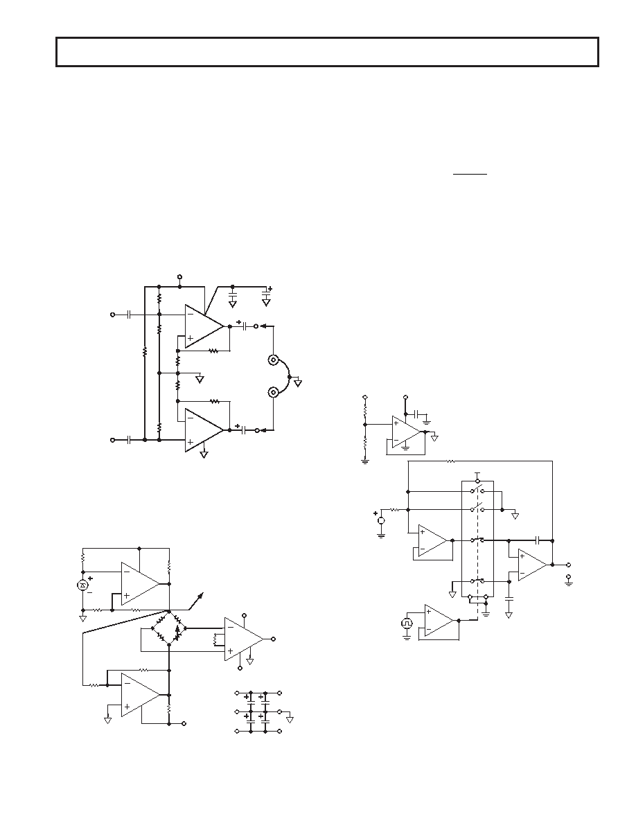
3 Volt, Single Supply Stereo Headphone Driver
The AD824 exhibits good current drive and THD+N perfor-
mance, even at 3 V single supplies. At 1 kHz, total harmonic
distortion plus noise (THD+N) equals –62 dB (0.079%) for a
300 mV p-p output signal. This is comparable to other single
supply op amps that consume more power and cannot run on 3 V
power supplies.
In Figure 6, each channel’s input signal is coupled via a 1
mF
Mylar capacitor. Resistor dividers set the dc voltage at the
noninverting inputs so that the output voltage is midway between
the power supplies (1.5 V). The gain is 1.5. Each half of the
AD824 can then be used to drive a headphone channel. A 5 Hz
high-pass filter is realized by the 500
mF capacitors and the
headphones, which can be modeled as 32 ohm load resistors to
ground. This ensures that all signals in the audio frequency
range (20 Hz–20 kHz) are delivered to the headphones.
MYLAR
1 F
1/4
AD824
L
R
HEADPHONES
32
IMPEDANCE
MYLAR
1/4
AD824
3V
0.1 F
CHANNEL 1
CHANNEL 2
1/4
AD824
47.5k
95.3k
0.1 F
500 F
4.99k
10k
47.5k
1 F
95.3k
4.99k
1/4
AD824
Figure 6. 3 Volt Single Supply Stereo Headphone Driver
Low Dropout Bipolar Bridge Driver
The AD824 can be used for driving a 350 ohm Wheatstone
bridge. Figure 7 shows one half of the AD824 being used to
buffer the AD589—a 1.235 V low power reference. The output
350
VREF
–VS
+VS
AD620
RG
R2
20
–4.5V
10k
26.4k , 1%
R1
20
TO A/D CONVERTER
REFERENCE INPUT
AD589
+1.235V
+5V
1 F
GND
+VS
–VS
0.1 F
–5V
1 F
0.1 F
1%
1/4
AD824
1/4
AD824
–VS
+VS
7
6
5
4
3
2
AD824
1/4
AD824
49.9k
1/4
AD824
Figure 7. Low Dropout Bipolar Bridge Driver
of 4.5 V can be used to drive an A/D converter front end. The
other half of the AD824 is configured as a unity-gain inverter
and generates the other bridge input of –4.5 V. Resistors R1 and
R2 provide a constant current for bridge excitation. The AD620
low power instrumentation amplifier is used to condition the
differential output voltage of the bridge. The gain of the AD620
is programmed using an external resistor RG and determined by:
G
=
49.4 k
W
RG
+ 1
A 3.3 V/5 V Precision Sample-and-Hold Amplifier
In battery-powered applications, low supply voltage operational
amplifiers are required for low power consumption. Also, low
supply voltage applications limit the signal range in precision
analog circuitry. Circuits like the sample-and-hold circuit shown
in Figure 8, illustrate techniques for designing precision analog
circuitry in low supply voltage applications. To maintain high
signal-to-noise ratios (SNRs) in a low supply voltage application
requires the use of rail-to-rail, input/output operational amplifi-
ers. This design highlights the ability of the AD824 to operate
rail-to-rail from a single 3 V/5 V supply, with the advantages of
high input impedance. The AD824, a quad JFET-input op amp,
is well suited to S/H circuits due to its low input bias currents
(3 pA, typical) and high input impedances (3
1013 W, typical).
The AD824 also exhibits very low supply currents so the total
supply current in this circuit is less than 2.5 mA.
\
3.3/5V
R1
50k
R2
50k
A1
3
2
4
1
11
0.1 F
FALSE GROUND (FG)
A4
12
13
14
SAMPLE/
HOLD
A3
10
9
8
A2
5
6
7
15
14
16
10
9
11
AD824B
3.3/5V
ADG513
R5
2k
AD824C
+
–
VOUT
CH
C
500pF
FG
4
5
8
6
7
2
3
1
AD824A
AD824D
R4
2k
FG
13
500pF
FG
A1
A2
A3
A4
Figure 8. 3.3 V/5.5 V Precision Sample and Hold
In many single supply applications, the use of a false ground
generator is required. In this circuit, R1 and R2 divide the
supply voltage symmetrically, creating the false ground voltage
at one-half the supply. Amplifier A1 then buffers this voltage
creating a low impedance output drive. The S/H circuit is con-
figured in an inverting topology centered around this false
ground level.
相关PDF资料 |
PDF描述 |
|---|---|
| AD824AR-14-3V-REEL | IC OPAMP JFET R-R 2MHZ LP 14SOIC |
| MCP6041-E/P | IC OPAMP 1.4V SNGL R-R 8DIP |
| MCP6041-E/MS | IC OPAMP 1.4V SNGL R-R 8MSOP |
| MCP6141T-E/SN | IC OPAMP 1.4V SNGL R-R 8SOIC |
| LRC-LRF2010LF-01-R020-F | RES .020 OHM 1W 1% 2010 SMD |
相关代理商/技术参数 |
参数描述 |
|---|---|
| AD824AR-14-REEL7 | 功能描述:IC OPAMP JFET R-R 2MHZ LP 14SOIC RoHS:否 类别:集成电路 (IC) >> Linear - Amplifiers - Instrumentation 系列:- 标准包装:150 系列:- 放大器类型:音频 电路数:2 输出类型:- 转换速率:5 V/µs 增益带宽积:12MHz -3db带宽:- 电流 - 输入偏压:100nA 电压 - 输入偏移:500µV 电流 - 电源:6mA 电流 - 输出 / 通道:50mA 电压 - 电源,单路/双路(±):4 V ~ 32 V,±2 V ~ 16 V 工作温度:-40°C ~ 85°C 安装类型:表面贴装 封装/外壳:8-TSSOP(0.173",4.40mm 宽) 供应商设备封装:8-TSSOP 包装:管件 |
| AD824AR-16 | 制造商:Analog Devices 功能描述: 制造商:Rochester Electronics LLC 功能描述: 制造商:Analog Devices 功能描述:QUAD OP-AMP, 4000 uV OFFSET-MAX, 2 MHz BAND WIDTH, PDSO16 |
| AD824AR-16-REEL | 制造商:Analog Devices 功能描述:OP Amp Quad GP R-R O/P ±15V/30V 16-Pin SOIC N T/R |
| AD824AR-3V | 制造商:AD 制造商全称:Analog Devices 功能描述:Single Supply, Rail-to-Rail Low Power, FET-Input Op Amp |
| AD824ARZ-14 | 功能描述:IC OPAMP JFET R-R 2MHZ LP 14SOIC RoHS:是 类别:集成电路 (IC) >> Linear - Amplifiers - Instrumentation 系列:- 标准包装:2,500 系列:- 放大器类型:通用 电路数:4 输出类型:- 转换速率:0.6 V/µs 增益带宽积:1MHz -3db带宽:- 电流 - 输入偏压:45nA 电压 - 输入偏移:2000µV 电流 - 电源:1.4mA 电流 - 输出 / 通道:40mA 电压 - 电源,单路/双路(±):3 V ~ 32 V,±1.5 V ~ 16 V 工作温度:0°C ~ 70°C 安装类型:表面贴装 封装/外壳:14-TSSOP(0.173",4.40mm 宽) 供应商设备封装:14-TSSOP 包装:带卷 (TR) 其它名称:LM324ADTBR2G-NDLM324ADTBR2GOSTR |
发布紧急采购,3分钟左右您将得到回复。