- 您现在的位置:买卖IC网 > PDF目录2137 > AD8260ACPZ-WP (Analog Devices Inc)IC AMP VGA DIFF LN 310MA 32LFCSP PDF资料下载
参数资料
| 型号: | AD8260ACPZ-WP |
| 厂商: | Analog Devices Inc |
| 文件页数: | 1/32页 |
| 文件大小: | 0K |
| 描述: | IC AMP VGA DIFF LN 310MA 32LFCSP |
| 标准包装: | 36 |
| 放大器类型: | 可变增益 |
| 电路数: | 1 |
| 输出类型: | 差分 |
| 转换速率: | 730 V/µs |
| -3db带宽: | 195MHz |
| 电流 - 输入偏压: | 200nA |
| 电流 - 电源: | 28.3mA |
| 电流 - 输出 / 通道: | 310mA |
| 电压 - 电源,单路/双路(±): | 3.3 V ~ 10 V,±3.3 V ~ 5 V |
| 工作温度: | -40°C ~ 105°C |
| 安装类型: | 表面贴装 |
| 封装/外壳: | 32-VFQFN 裸露焊盘,CSP |
| 供应商设备封装: | 32-LFCSP-VQ |
| 包装: | 托盘 - 晶粒 |
| 配用: | AD8260-EVALZ-ND - BOARD EVAL FOR AD8260 |
当前第1页第2页第3页第4页第5页第6页第7页第8页第9页第10页第11页第12页第13页第14页第15页第16页第17页第18页第19页第20页第21页第22页第23页第24页第25页第26页第27页第28页第29页第30页第31页第32页
High Current Driver Amplifier and
Digital VGA/Preamplifier with 3 dB Steps
AD8260
Rev. A
Information furnished by Analog Devices is believed to be accurate and reliable. However, no
responsibilityisassumedbyAnalogDevicesforitsuse,norforanyinfringementsofpatentsorother
rightsofthirdpartiesthatmayresultfromitsuse.Specificationssubjecttochangewithoutnotice.No
license is granted by implication or otherwise under any patent or patent rights of Analog Devices.
Trademarksandregisteredtrademarksarethepropertyoftheirrespectiveowners.
One Technology Way, P.O. Box 9106, Norwood, MA 02062-9106, U.S.A.
Tel: 781.329.4700
Fax: 781.461.3113
2008–2011 Analog Devices, Inc. All rights reserved.
FEATURES
High current driver
Differential input—direct drive from DAC
Preset gain: 1.5×
3 dB bandwidth: 195 MHz
Large output drive: >±300 mA
VGA/preamplifier
Low noise
Voltage noise: 2.4 nV/√Hz
Current noise: 5 pA/√Hz
3 dB bandwidth: 230 MHz
Gain range: 30 dB in 3 dB steps
6 dB to +24 dB (for preamplifier gain of 6 dB)
Single-ended preamplifier input and differential VGA
output
Supplies: 3.3 V to 10 V (with VMID enabled)
±3.3 V to ±5 V (with VMID disabled)
Power: 93 mW with 3.3 V supplies
Power-down for VGA, driver amplifier, and system
APPLICATIONS
Digital AGC systems
Tx/Rx signal processing
Power line transceivers
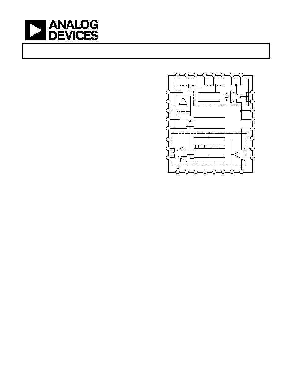
FUNCTIONAL BLOCK DIAGRAM
32
2
3
6
31
30
1.5k
1k
29
28
27
26
25
1k
1.5k
GM
HIGH CURRENT DRIVER
9
24
23
22
21
VMID
4
1
AD8260
VMDO
TXEN
VMDI
VNCM
VPSB
ENBL
VGAP
VGAN
VNGR VPSR GNS3 GNS2 GNS1 GNS0 PRAO VNGR
VOCM INPP INRP INRN INPN TXFB VNEG
VNEG
TXOP
VPOS
VPSR
VMDO
PRAI
FDBK
07192-
001
5
7
8
10
11
12
13
14
16
15
17
18
19
20
BIAS
VGA/PREAMPLIFIER
ATTENUATOR
GM STAGES
LOGIC
×1
+
–
Figure 1. Functional Block Diagram
GENERAL DESCRIPTION
The AD8260 includes a high current driver, usable as a
transmitter, and a low noise digitally programmable variable
gain amplifier (DGA), useable as a receiver.
The receiver section consists of a single-ended input preampli-
fier, and linear-in-dB, differential-output DGA. The receiver has
a small signal –3 dB bandwidth of 230 MHz; the driver small
signal bandwidth is 195 MHz. The driver delivers ±300 mA,
well suited for driving low impedance loads, even when
connected to a 3.3 V supply.
The AD8260 DGA is ideal for trim applications and has a gain
span of 30 dB, in 3 dB steps. Excellent bandwidth uniformity is
maintained across the entire frequency range. The low output-
referred noise of the DGA is advantageous in driving high
speed ADCs. The differential output facilitates the interface to
modern low voltage high speed ADCs.
Single-supply and dual-supply operation makes the part versatile
and enables gain control of negative-going pulses, such as those
generated by photodiodes or photo-multiplier tubes, as well as
processing band-pass signals on a single supply. For maximum
dynamic range, it is essential that the part be ac-coupled when
operating on a single supply.
The AD8260 preamplifier (PrA) is configured with external
resistors for gains greater than 6 dB and can be inverting or
noninverting. The DGA is characterized with a noninverting
preamplifier gain of 2×. The attenuator has a range of 30 dB and
the output amplifier has a gain of 8× (18.06 dB). The lowest
noninverting gain range is 6 dB to +24 dB and shifts up with
increased preamplifier gain. The gain is controlled via a parallel
port (Pin GNS0 to Pin GNS3) with 10 gain steps of 3 dB per
code. The preamplifier and DGA are disabled for any code that
is not assigned a gain step.
The AD8260 can operate with single or dual supplies from 3.3 V
to ±5 V. An internal buffer normally provides a split supply
reference for single-supply operation; an external reference
can also be used when the VMID buffer is shut down.
The operating temperature range is 40°C to +105°C. The
AD8260 is available in a 5 mm × 5 mm, 32-lead LFCSP.
相关PDF资料 |
PDF描述 |
|---|---|
| AD8264ACPZ-R7 | IC AMP VGA DIFF QUAD LN 40LFCSP |
| AD826AR-REEL7 | IC OPAMP VF 50MHZ DUAL LP 8SOIC |
| AD8270ACPZ-R7 | IC AMP DIFF 20MHZ DUAL 16LFCSP |
| AD8271BRMZ-R7 | IC AMP PGA 15MHZ LDIST 10MSOP |
| AD8273ARZ-R7 | IC AMP AUDIO 2CH DIFF 14SOIC |
相关代理商/技术参数 |
参数描述 |
|---|---|
| AD8260-EVALZ | 功能描述:BOARD EVAL FOR AD8260 RoHS:是 类别:编程器,开发系统 >> 评估板 - 运算放大器 系列:- 产品培训模块:Lead (SnPb) Finish for COTS Obsolescence Mitigation Program 标准包装:1 系列:- |
| AD8264 | 制造商:AD 制造商全称:Analog Devices 功能描述:Quad, 235 MHz, DC-Coupled VGA and Differential Output Amplifier |
| AD8264ACPZ | 功能描述:IC AMP VGA DIFF QUAD LN 40LFCSP RoHS:是 类别:集成电路 (IC) >> Linear - Amplifiers - Instrumentation 系列:- 标准包装:1 系列:- 放大器类型:通用 电路数:4 输出类型:满摆幅 转换速率:0.028 V/µs 增益带宽积:105kHz -3db带宽:- 电流 - 输入偏压:3nA 电压 - 输入偏移:100µV 电流 - 电源:3.3µA 电流 - 输出 / 通道:12mA 电压 - 电源,单路/双路(±):2.7 V ~ 12 V,±1.35 V ~ 6 V 工作温度:-40°C ~ 85°C 安装类型:表面贴装 封装/外壳:14-TSSOP(0.173",4.40mm 宽) 供应商设备封装:14-TSSOP 包装:剪切带 (CT) 其它名称:OP481GRUZ-REELCT |
| AD8264ACPZ-R7 | 功能描述:IC AMP VGA DIFF QUAD LN 40LFCSP RoHS:是 类别:集成电路 (IC) >> Linear - Amplifiers - Instrumentation 系列:- 标准包装:50 系列:- 放大器类型:J-FET 电路数:2 输出类型:- 转换速率:3.5 V/µs 增益带宽积:1MHz -3db带宽:- 电流 - 输入偏压:30pA 电压 - 输入偏移:2000µV 电流 - 电源:200µA 电流 - 输出 / 通道:- 电压 - 电源,单路/双路(±):7 V ~ 36 V,±3.5 V ~ 18 V 工作温度:0°C ~ 70°C 安装类型:通孔 封装/外壳:8-DIP(0.300",7.62mm) 供应商设备封装:8-PDIP 包装:管件 |
| AD8264ACPZ-RL | 功能描述:IC AMP VGA DIFF QUAD LN 40LFCSP RoHS:是 类别:集成电路 (IC) >> Linear - Amplifiers - Instrumentation 系列:- 标准包装:2,500 系列:Excalibur™ 放大器类型:J-FET 电路数:1 输出类型:- 转换速率:45 V/µs 增益带宽积:10MHz -3db带宽:- 电流 - 输入偏压:20pA 电压 - 输入偏移:490µV 电流 - 电源:1.7mA 电流 - 输出 / 通道:48mA 电压 - 电源,单路/双路(±):4.5 V ~ 38 V,±2.25 V ~ 19 V 工作温度:-40°C ~ 85°C 安装类型:表面贴装 封装/外壳:8-SOIC(0.154",3.90mm 宽) 供应商设备封装:8-SOIC 包装:带卷 (TR) |
发布紧急采购,3分钟左右您将得到回复。