- 您现在的位置:买卖IC网 > PDF目录16923 > AD8264-EVALZ (Analog Devices Inc)BOARD EVAL FOR AD8264 VGA PDF资料下载
参数资料
| 型号: | AD8264-EVALZ |
| 厂商: | Analog Devices Inc |
| 文件页数: | 25/40页 |
| 文件大小: | 0K |
| 描述: | BOARD EVAL FOR AD8264 VGA |
| 标准包装: | 1 |
| 每 IC 通道数: | 4 - 四 |
| 放大器类型: | 可变增益 |
| 输出类型: | 差分 |
| 转换速率: | 380 V/µs |
| -3db带宽: | 235MHz |
| 工作温度: | -40°C ~ 105°C |
| 电流供应(主 IC): | 99mA |
| 电压 - 电源,单路/双路(±): | ±2.5 V ~ 5 V |
| 板类型: | 完全填充 |
| 已供物品: | 板 |
| 已用 IC / 零件: | AD8264 |
第1页第2页第3页第4页第5页第6页第7页第8页第9页第10页第11页第12页第13页第14页第15页第16页第17页第18页第19页第20页第21页第22页第23页第24页当前第25页第26页第27页第28页第29页第30页第31页第32页第33页第34页第35页第36页第37页第38页第39页第40页
AD8264
Rev. A | Page 31 of 40
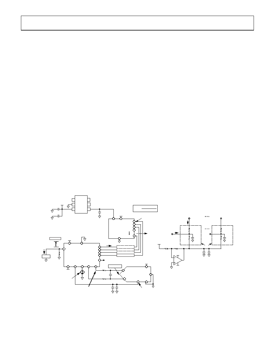
A DC CONNECTED CONCEPT EXAMPLE
The dc connected concept example in Figure 113 is an application
with the 40-channel AD5381, 3 V, 12-bit DAC. The main difference
between this example and Figure 112 is that, for the same ADR127
1.25 V reference, the full-scale output of the DAC is from
0 V to 2 × VREFIN = 2.5 V. Two options for gain control
include the following:
Use the same circuit as in Figure 112 but use only half the
DAC output voltage from 0 V to 1.25 V. This is the simplest
solution, requiring the fewest extra components. Note that
the overall gain resolution increases by one bit to 11 bits
over the 10-bit AD5314.
Ground GNLO and scale the DAC output so that the
GNHx inputs vary from 0.652 V to +0.625 V. Figure 113
shows a possible circuit implementation using a divider
between the DAC output and a 1.25 V reference.
GNLO cannot simply be increased to 1.25 V because, for a
given supply voltage, GNLO has a limited voltage range to
achieve the full gain span (see Table 5).
However, a third possibility is to use another voltage that is
between 1.2 V and 625 mV on GNLO, such as 1 V. In this case,
the DAC must vary from 0.375 V to 1.625 V to achieve the fully
specified gain range.
Note the gain limits when the differential gain control exceeds
±0.625 V, either to 6 dB or to 30 dB. If the differential gain
control input voltage is exceeded, no gain foldover occurs.
Figure 113 shows how the AD8264 is connected in a PET
application. The PMT generates a negative-going current pulse
that results in a voltage pulse at the preamplifier input and a
differential output pulse on VOLx and VOHx.
To fully appreciate the advantages of the AD8264, note the
common-mode and polarity conversion afforded. The AD9228,
as with most modern ADCs, is a low voltage, single-polarity
device. Recall that the PMT is a high voltage device that yields a
negative pulse. To map the pulse to the input range of the ADC,
the pulse must be inverted, shifted, and amplified to the full
input range of the ADC. This is done by using the gain control,
signal offset, and common-mode features of the AD8264.
The full-scale input of the converter is 0 V to 2 V, with a common-
mode of 1 V. Match the VOCM voltage of the AD8264 to the
ADC common mode (VREF = 1 V), and the two devices can be
connected directly using an appropriate level of the antialiasing
filter. The PMT signal is 0 V to 0.1 V. With a gain of 20× (26 dB),
the AD8264 output signal range is 2 V p-p. Prebias the signal
negative by 0.5 V using the AD8264 OFSx inputs, which sets
VOHx = 1.5 V and VOLx = 0.5 V for VOCM = 1 V. The output
is perfectly matched to the input of the ADC.
Note that, by connecting VOLx to the positive ADC input and
VOHx to the negative ADC input, the negative input pulse is
inverted automatically. The VGAx output is still a negative
pulse, amplified by 20 dB for this example.
+3.3V
–3.3V
0.1F
NC 6
NC 5
VOUT 4
1
2
3
NC
GND
VIN
ADR127
REFIN
DAC
AD5381
GND
2 × VREFIN × D
VOUT =
2N
10F
VREF = 1.25V
GNH1
GNH2
GNH3
GNH4
AD8264
GNLO
VOUT RANGE = 0V TO 1.25V
EACH
VOCM
VOHx VOLx
VDD
RFILT
CFILT
ADC
AD9222/
AD9228
VREF
VDD
+1.8V
SENSE
GND
VIN + x
VIN – x
SENSE GROUNDED: VREF = 1V
VNEG
VPOS
IPPx
100
OFSx
~250nA EACH
VGAx
VGA OUTPUTS TO OTHER
SIGNAL PROCESSING
OUTPUT COMMON-MODE VOLTAGE = 1V
VOHx = 1.5V, VOLx = 0.5V; VOFx = –0.5V
FS = 2V p-p
1F
0.1F
10F
+3.3V
PMT
0V
–0.1V
EXAMPLE
VOFS = –0.5V
SCALE
CIRCUIT
VOUT0
VOUT1
VOUT2
VOUT4
VOUT39
TO 9 OTHER
AD8264s
SCALE CIRCUIT
+3.3V
–3.3V
VOLTAGE FROM DAC AD5381 = 0 TO 2.5V
VARIES FROM
12.5 TO 32.5A
~250nA
VREF = 1.25V
AD8663
49.9k
1%
VOUT0
VOUT39
GNH1
SCALE CIRCUIT
–1.25V
GNH4
–625mV
TO
+625mV
49.9k
1%
49.9k
1%
0.1F
49.9k
1%
49.9k
1%
0.1F
10F
49.9k
1%
07736-
083
Figure 113. Concept Application of AD8264 with 40-Channel AD5381 12-Bit, 3 V DAC and AD9222/AD9228 12-Bit ADC
相关PDF资料 |
PDF描述 |
|---|---|
| X60003BIG3Z-50T1 | IC VREF SERIES PREC 5V SOT-23-3 |
| 381LX471M450A052 | CAP ALUM 470UF 450V 20% SNAP |
| 1-556127-2 | CABLE ASSY PWR-PWR 8 WIRE 116" |
| AD8337-EVALZ-INV | BOARD EVALUATION FOR AD8337 INS |
| EBM30DCTS | CONN EDGECARD 60POS DIP .156 SLD |
相关代理商/技术参数 |
参数描述 |
|---|---|
| AD826AN | 制造商:Analog Devices 功能描述:OP Amp Dual Volt Fdbk 制造商:Rochester Electronics LLC 功能描述:DUAL, HIGH SPEED OP AMP - Bulk 制造商:Analog Devices 功能描述:Operational Amplifier (Op-Amp) IC |
| AD826ANZ | 功能描述:IC OPAMP VF 50MHZ DUAL LP 8DIP RoHS:是 类别:集成电路 (IC) >> Linear - Amplifiers - Instrumentation 系列:- 标准包装:2,500 系列:- 放大器类型:通用 电路数:4 输出类型:- 转换速率:0.6 V/µs 增益带宽积:1MHz -3db带宽:- 电流 - 输入偏压:45nA 电压 - 输入偏移:2000µV 电流 - 电源:1.4mA 电流 - 输出 / 通道:40mA 电压 - 电源,单路/双路(±):3 V ~ 32 V,±1.5 V ~ 16 V 工作温度:0°C ~ 70°C 安装类型:表面贴装 封装/外壳:14-TSSOP(0.173",4.40mm 宽) 供应商设备封装:14-TSSOP 包装:带卷 (TR) 其它名称:LM324ADTBR2G-NDLM324ADTBR2GOSTR |
| AD826ANZ | 制造商:Analog Devices 功能描述:Operational Amplifier (Op-Amp) IC |
| AD826AR | 功能描述:IC OPAMP VF 50MHZ DUAL LP 8SOIC RoHS:否 类别:集成电路 (IC) >> Linear - Amplifiers - Instrumentation 系列:- 标准包装:50 系列:- 放大器类型:J-FET 电路数:2 输出类型:- 转换速率:13 V/µs 增益带宽积:3MHz -3db带宽:- 电流 - 输入偏压:65pA 电压 - 输入偏移:3000µV 电流 - 电源:1.4mA 电流 - 输出 / 通道:- 电压 - 电源,单路/双路(±):7 V ~ 36 V,±3.5 V ~ 18 V 工作温度:-40°C ~ 85°C 安装类型:通孔 封装/外壳:8-DIP(0.300",7.62mm) 供应商设备封装:8-PDIP 包装:管件 |
| AD826AR-EBZ | 功能描述:BOARD EVAL FOR AD826AR OPAMP RoHS:是 类别:编程器,开发系统 >> 评估板 - 运算放大器 系列:- 产品培训模块:Lead (SnPb) Finish for COTS Obsolescence Mitigation Program 标准包装:1 系列:- |
发布紧急采购,3分钟左右您将得到回复。