参数资料
| 型号: | AD8306AR |
| 厂商: | Analog Devices Inc |
| 文件页数: | 16/16页 |
| 文件大小: | 0K |
| 描述: | IC LOGARITHM AMP 5-400MHZ 16SOIC |
| 标准包装: | 1 |
| 类型: | 限制-对数放大器 |
| 应用: | 接收器信号强度指示(RSSI) |
| 安装类型: | 表面贴装 |
| 封装/外壳: | 16-SOIC(0.154",3.90mm 宽) |
| 供应商设备封装: | 16-SO |
| 包装: | 管件 |
REV. A
AD8306
–9–
the intercept to –108 dBV, by raising the RSSI output voltage for
zero input, and to provide temperature compensation, resulting
in a stable intercept. For zero signal conditions, all the detector
output currents are equal. For a finite input, of either polarity,
their difference is converted by the output interface to a single-
sided voltage nominally scaled 20 mV/dB (400 mV per decade), at
the output VLOG (Pin 16). This scaling is controlled by a sepa-
rate feedback stage, having a tightly controlled transcon-
ductance. A small uncertainty in the log slope and intercept
remains (see Specifications); the intercept may be adjusted (see
Applications).
VPS2
FLTR
VLOG
20mV/dB
COMM
ISOURCE
>50mA
ON DEMAND
C1
3.5pF
CURRENT
MIRROR
ISINK
FIXED
1mA
3.3k
125 A
1.3k
TRANSCONDUCTANCE
DETERMINES SLOPE
IT
LGP
LGN
SUMMED
DETECTOR
OUTPUTS
CF
250 s
VLOG
Figure 23. Simplified RSSI Output Interface
The RSSI output bandwidth, fLP, is nominally 3.5 MHz. This is
controlled by the compensation capacitor C1, which may be
increased by adding an external capacitor, CF, between FLTR
(Pin 10) and VLOG (Pin 16). An external 33 pF will reduce fLP
to 350 kHz, while 360 pF will set it to 35 kHz, in each case with
an essentially one-pole response. In general, the relationships
(for fLP in MHz) are:
C
f
pF
f
CpF
F
LP
F
=
×
=
×
+
12 7 10
35
12 7 10
35
10
6
.
–.
;
.
–
(1)
Using a load resistance of 50
or greater, and at any tempera-
ture, the peak output voltage may be at least 2.4 V when using a
supply of 4.5 V, and at least 2.1 V for a 3 V supply, which is
consistent with the maximum permissible input levels. The incre-
mental output resistance is approximately 0.3
at low frequen-
cies, rising to 1
at 150 kHz and 18 at very high frequencies.
The output is unconditionally stable with load capacitance, but
it should be noted that while the peak sourcing current is
over 100 mA, and able to rapidly charge even large capacitances,
the internally provided sinking current is only 1 mA. Thus, the
fall time from the 2 V level will be as long as 2
s for a 1 nF
load. This may be reduced by adding a grounded load resistance.
USING THE AD8306
The AD8306 exhibits very high gain from 1 MHz to over 1 GHz,
at which frequency the gain of the main path is still over 65 dB.
Consequently, it is susceptible to all signals, within this very
broad frequency range, that find their way to the input termi-
nals. It is important to remember that these are quite indistin-
guishable from the “wanted” signal, and will have the effect of
raising the apparent noise floor (that is, lowering the useful
dynamic range). Therefore, while the signal of interest may be
an IF of, say, 200 MHz, any of the following could easily be
larger than this signal at the lower extremities of its dynamic
range: a 60 Hz hum, picked up due to poor grounding tech-
niques; spurious coupling from digital logic on the same PC
board; a strong EMI source; etc.
Very careful shielding is essential to guard against such un-
wanted signals, and also to minimize the likelihood of instability
due to HF feedback from the limiter outputs to the input. With
this in mind, the minimum possible limiter gain should be used.
Where only the logarithmic amplifier (RSSI) function is re-
quired, the limiter should be disabled by omitting RLIM and
tying the outputs LMHI and LMLO directly to VPS2. A good
ground plane should be used to provide a low impedance con-
nection to the common pins, for the decoupling capacitor(s)
used at VPS1 and VPS2, and at the output ground. Note that
COM2 is a special ground pin serving just the RSSI output.
The four pins labeled PADL tie down directly to the metallic
lead frame, and are thus connected to the back of the chip. The
process on which the AD8306 is fabricated uses a bonded-wafer
technique to provide a silicon-on-insulator isolation, and there is
no junction or other dc path from the back side to the circuitry
on the surface. These paddle pins must be connected directly to
the ground plane using the shortest possible lead lengths to
minimize inductance.
The voltages at the two supply pins should not be allowed to
differ greatly; up to 500 mV is permissible. It is desirable to
allow VPS1 to be slightly more negative than VPS2. When the
primary supply is greater than 2.7 V, the decoupling resistors R1
and R2 (Figure 24) may be increased to improve the isolation
and lower the dissipation in the IC. However, since VPS2 sup-
ports the RSSI load current, which may be large, the value of
R2 should take this into account.
Basic Connections for Log (RSSI) Output
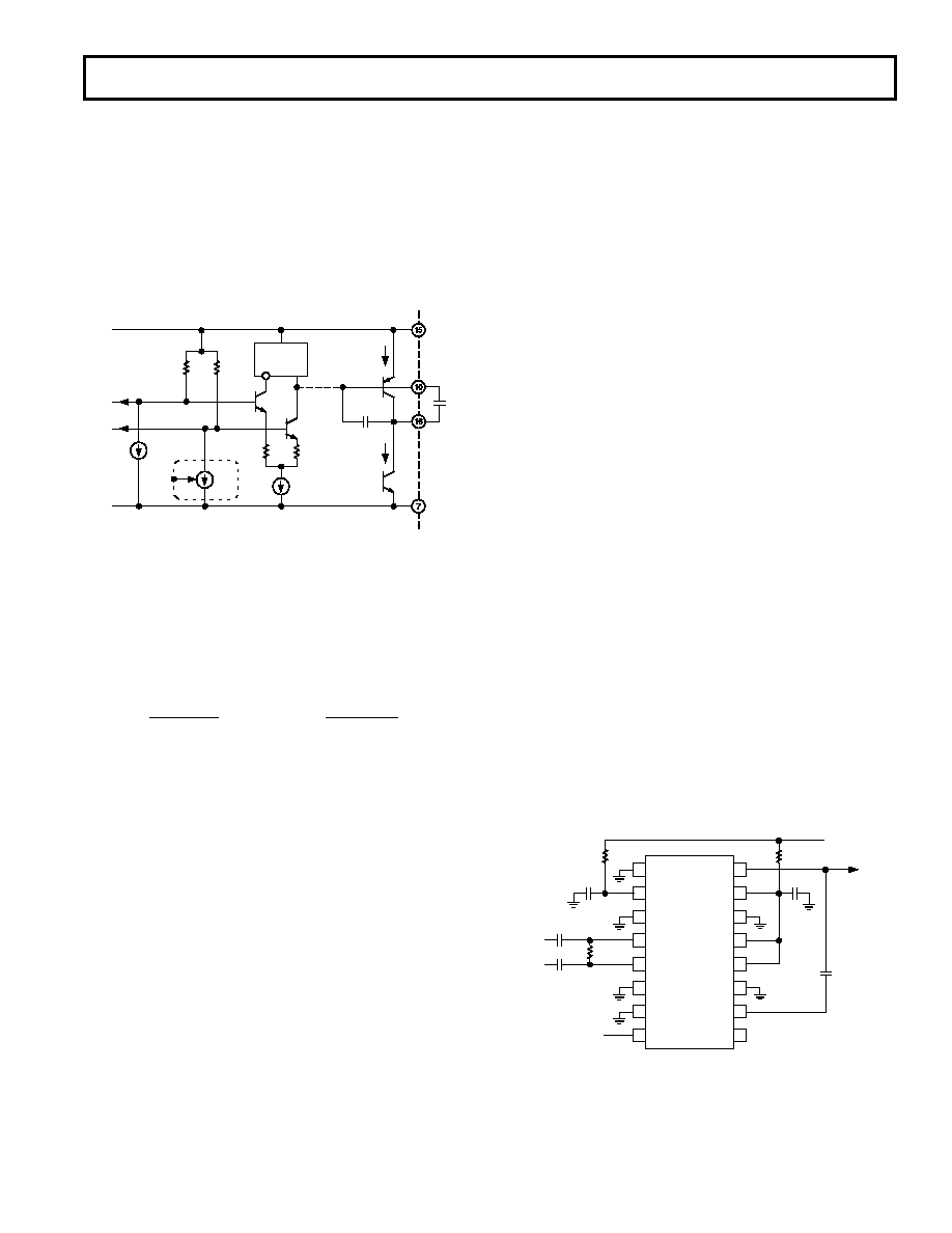
Figure 24 shows the connections required for most applications.
The AD8306 is enabled by connecting ENBL to VPS1. The
device is put into the sleep mode by grounding this pin. The
inputs are ac-coupled by C1 and C2, which normally should
have the same value (CC). The input is, in this case, terminated
with a 52.3
resistor that combines with the AD8306’s input
resistance of 1000
to give a broadband input impedance of
50
. Alternatively an input matching network can be used (see
Input Matching section).
1
2
3
4
5
6
7
8
VLOG
VPS2
PADL
LMHI
LMLO
PADL
FLTR
LMDR
COM2
VPS1
PADL
INHI
INLO
PADL
COM1
ENBL
AD8306
9
10
11
14
15
16
0.1 F
R2
10
RSSI
0.1 F
R1
10
ENABLE
RT
52.3
C1
0.01 F
SIGNAL
INPUTS
12
13
VS (2.7V TO 6.5V)
C2
0.01 F
CF
(OPTIONAL
SEE TEXT)
Figure 24. Basic Connections for RSSI (Log) Output
The 0.01
F coupling capacitors and the resulting 50 input
impedance give a high-pass corner frequency of around 600 kHz.
(1/
(2 π RC)), where C = (C1)/2. In high frequency applications,
this corner frequency should be placed as high as possible, to
minimize the coupling of unwanted low frequency signals. In
相关PDF资料 |
PDF描述 |
|---|---|
| AD8307AN | IC LOGARITHMIC AMP 8-DIP |
| AD8309ARU | IC LOGARITHM AMP 100DB 16-TSSOP |
| AD830ANZ | IC VIDEO DIFF AMP HS 8-DIP |
| AD8310ARM | IC LOGARITHMIC AMP 95DB 8-MSOP |
| AD8317ACPZ-R7 | IC AMP LOG DETECT 8GHZ 8-LFCSP |
相关代理商/技术参数 |
参数描述 |
|---|---|
| AD8306AR-REEL | 制造商:Analog Devices 功能描述:SP Amp LOG Amp Single 6.5V 16-Pin SOIC N T/R |
| AD8306AR-REEL7 | 功能描述:IC LOG-LIMITING AMP HP 16-SOIC RoHS:否 类别:集成电路 (IC) >> 线性 - 放大器 - 专用 系列:- 产品培训模块:Lead (SnPb) Finish for COTS Obsolescence Mitigation Program 标准包装:60 系列:- 类型:可变增益放大器 应用:CATV 安装类型:表面贴装 封装/外壳:20-WQFN 裸露焊盘 供应商设备封装:20-TQFN-EP(5x5) 包装:托盘 |
| AD8306ARZ | 功能描述:IC LOG-LIMITING AMP 16-SOIC RoHS:是 类别:集成电路 (IC) >> 线性 - 放大器 - 专用 系列:- 产品培训模块:Lead (SnPb) Finish for COTS Obsolescence Mitigation Program 标准包装:60 系列:- 类型:可变增益放大器 应用:CATV 安装类型:表面贴装 封装/外壳:20-WQFN 裸露焊盘 供应商设备封装:20-TQFN-EP(5x5) 包装:托盘 |
| AD8306ARZ | 制造商:Analog Devices 功能描述:Logarithmic Amplifier IC |
| AD8306ARZ-REEL | 制造商:Analog Devices 功能描述:SP Amp LOG Amp Single 6.5V 16-Pin SOIC N T/R 制造商:Analog Devices 功能描述:SP AMP LOG AMP SGL 6.5V 16SOIC N - Tape and Reel |
发布紧急采购,3分钟左右您将得到回复。