参数资料
| 型号: | AD8306AR |
| 厂商: | Analog Devices Inc |
| 文件页数: | 2/16页 |
| 文件大小: | 0K |
| 描述: | IC LOGARITHM AMP 5-400MHZ 16SOIC |
| 标准包装: | 1 |
| 类型: | 限制-对数放大器 |
| 应用: | 接收器信号强度指示(RSSI) |
| 安装类型: | 表面贴装 |
| 封装/外壳: | 16-SOIC(0.154",3.90mm 宽) |
| 供应商设备封装: | 16-SO |
| 包装: | 管件 |
REV. A
AD8306
–10–
low frequency applications, a simple RC network forming a low-
pass filter should be added at the input for the same reason.
If the limiter output is not required, Pin 9 (LMDR) should be
left open and Pins 12 and 13 (LMHI, LMLO) should be tied to
VPS2 as shown in Figure 24.
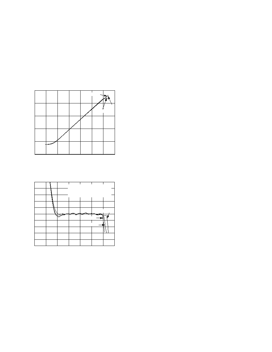
Figure 25 shows the output versus the input level in dBV, for
sine inputs at 10 MHz, 50 MHz and 100 MHz (add 13 to the
dBV number to get dBm Re 50
. Figure 26 shows the typi-
cal logarithmic linearity (log conformance) under the same
conditions.
INPUT LEVEL – dBV
2.5
–120
RSSI
OUTPUT
–
V
2
1.5
1
0.5
0
–100
–80
–60
–40
–20
0
20
100MHz
50MHz
10MHz
Figure 25. RSSI Output vs. Input Level at TA = +25°C for
Frequencies of 10 MHz, 50 MHz and 100 MHz
5
–120
ERROR
–
dB
4
3
2
1
0
–1
–2
–100
–80
–60
–40
–20
20
–3
–4
–5
–100
INPUT LEVEL – dBV
0
DYNAMIC RANGE
1dB
3dB
10MHz
86
93
50MHz
90
97
100MHz
96
100
100MHz
50MHz
10MHz
Figure 26. Log Linearity vs. Input Level at TA = +25°C, for
Frequencies of 10 MHz, 50 MHz and 100 MHz
Transfer Function in Terms of Slope and Intercept
The transfer function of the AD8306 is characterized in terms
of its Slope and Intercept. The logarithmic slope is defined as
the change in the RSSI output voltage for a 1 dB change at the
input. For the AD8306 the slope is calibrated to be 20 mV/dB.
The intercept is the point at which the extrapolated linear re-
sponse would intersect the horizontal axis. For the AD8306 the
intercept is calibrated to be –108 dBV (–95 dBm). Using the
slope and intercept, the output voltage can be calculated for any
input level within the specified input range using the equation:
VOUT = VSLOPE × (PIN – PO)
(2)
where VOUT is the demodulated and filtered RSSI output,
VSLOPE is the logarithmic slope, expressed in V/dB, PIN is the
input signal, expressed in decibels relative to some reference
level (either dBm or dBV in this case) and PO is the logarithmic
intercept, expressed in decibels relative to the same reference
level.
For example, for an input level of –33 dBV (–20 dBm), the
output voltage will be
VOUT = 0.02 V/dB × (–33 dBV – (–108 dBV)) = 1.5 V
(3)
The most widely used convention in RF systems is to specify
power in dBm, that is, decibels above 1 mW in 50
. Specifica-
tion of log amp input level in terms of power is strictly a conces-
sion to popular convention; they do not respond to power (tacitly
“power absorbed at the input”), but to the input voltage. The
use of dBV, defined as decibels with respect to a 1 V rms sine wave,
is more precise, although this is still not unambiguous because
waveform is also involved in the response of a log amp, which,
for a complex input (such as a CDMA signal) will not follow the
rms value exactly. Since most users specify RF signals in terms
of power—more specifically, in dBm/50
—we use both dBV
and dBm in specifying the performance of the AD8306, showing
equivalent dBm levels for the special case of a 50
environment.
Values in dBV are converted to dBm re 50
by adding 13.
Output Response Time and CF
The RSSI output has a low-pass corner frequency of 3.5 MHz,
which results in a 10% to 90% rise time of 73 ns. For low fre-
quency applications, the corner frequency can be reduced by
adding an external capacitor, CF, between FLTR (Pin 10) and
VLOG (Pin 16) as shown in Figure 24. For example, an exter-
nal 33 pF will reduce the corner frequency to 350 kHz, while
360 pF will set it to 35 kHz, in each case with an essentially
one-pole response.
Using the Limiter
Figure 27 shows the basic connections for operating the limiter
and the log output concurrently. The limiter output is a pair of
differential currents of magnitude, IOUT, from high impedance
(open-collector) sources. These are converted to equal-amplitude
voltages by supply-referenced load resistors, RLOAD. The limiter
output current is set by RLIM, the resistor connected between
Pin 9 (LMDR) and ground. The limiter output current is set
according the equation:
IOUT = –400 mV/RLIM
(5)
and has an absolute accuracy of
±5%.
The supply referenced voltage on each of the limiter pins will
thus be given by:
VLIM = VS –400 mV × RLOAD/RLIM
(6)
相关PDF资料 |
PDF描述 |
|---|---|
| AD8307AN | IC LOGARITHMIC AMP 8-DIP |
| AD8309ARU | IC LOGARITHM AMP 100DB 16-TSSOP |
| AD830ANZ | IC VIDEO DIFF AMP HS 8-DIP |
| AD8310ARM | IC LOGARITHMIC AMP 95DB 8-MSOP |
| AD8317ACPZ-R7 | IC AMP LOG DETECT 8GHZ 8-LFCSP |
相关代理商/技术参数 |
参数描述 |
|---|---|
| AD8306AR-REEL | 制造商:Analog Devices 功能描述:SP Amp LOG Amp Single 6.5V 16-Pin SOIC N T/R |
| AD8306AR-REEL7 | 功能描述:IC LOG-LIMITING AMP HP 16-SOIC RoHS:否 类别:集成电路 (IC) >> 线性 - 放大器 - 专用 系列:- 产品培训模块:Lead (SnPb) Finish for COTS Obsolescence Mitigation Program 标准包装:60 系列:- 类型:可变增益放大器 应用:CATV 安装类型:表面贴装 封装/外壳:20-WQFN 裸露焊盘 供应商设备封装:20-TQFN-EP(5x5) 包装:托盘 |
| AD8306ARZ | 功能描述:IC LOG-LIMITING AMP 16-SOIC RoHS:是 类别:集成电路 (IC) >> 线性 - 放大器 - 专用 系列:- 产品培训模块:Lead (SnPb) Finish for COTS Obsolescence Mitigation Program 标准包装:60 系列:- 类型:可变增益放大器 应用:CATV 安装类型:表面贴装 封装/外壳:20-WQFN 裸露焊盘 供应商设备封装:20-TQFN-EP(5x5) 包装:托盘 |
| AD8306ARZ | 制造商:Analog Devices 功能描述:Logarithmic Amplifier IC |
| AD8306ARZ-REEL | 制造商:Analog Devices 功能描述:SP Amp LOG Amp Single 6.5V 16-Pin SOIC N T/R 制造商:Analog Devices 功能描述:SP AMP LOG AMP SGL 6.5V 16SOIC N - Tape and Reel |
发布紧急采购,3分钟左右您将得到回复。