- 您现在的位置:买卖IC网 > PDF目录10572 > AD8321ARZ-REEL (Analog Devices Inc)IC LINE DVR CATV 20-SOIC T/R PDF资料下载
参数资料
| 型号: | AD8321ARZ-REEL |
| 厂商: | Analog Devices Inc |
| 文件页数: | 15/20页 |
| 文件大小: | 0K |
| 描述: | IC LINE DVR CATV 20-SOIC T/R |
| 产品变化通告: | AD8321 Discontinuation 02/Mar/2012 |
| 标准包装: | 1,000 |
| 类型: | 线路驱动器,发射器 |
| 应用: | 调制解调器,CATV |
| 安装类型: | 表面贴装 |
| 封装/外壳: | 20-SOIC(0.295",7.50mm 宽) |
| 供应商设备封装: | 20-SOIC W |
| 包装: | 带卷 (TR) |
| 配用: | AD8321-EVAL-ND - BOARD EVAL FOR AD8321 |
AD8321
ABSOLUTE MAXIMUM RATINGS
*
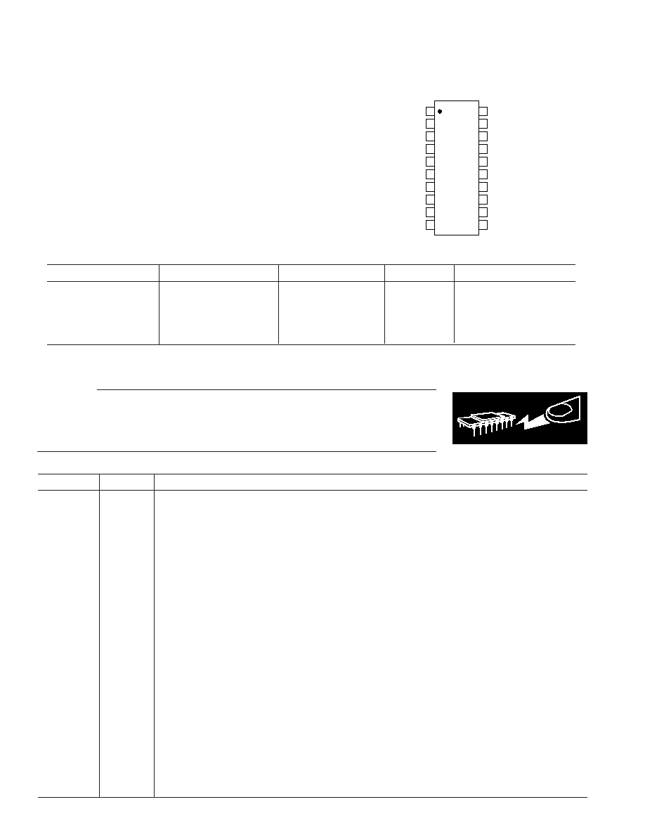
PIN CONFIGURATION
Supply Voltage +VS
Pins 7, 8, 9, 17, 20 . . . . . . . . . . . . . . . . . . . . . . . . . . . +11 V
Input Voltages
SDATA
Pins 18, 19 . . . . . . . . . . . . . . . . . . . . . . . . . . . . . . . .
±0.5 V
CLK
Pins 1, 2, 3, 6 . . . . . . . . . . . . . . . . . . . . . . . –0.8 V to +5.5 V
DATEN
Internal Power Dissipation
GND
Small Outline (R) . . . . . . . . . . . . . . . . . . . . . . . . . . . 0.90 W
BYP1
Operating Temperature Range . . . . . . . . . . . –40
∞C to +85∞C
PD
Storage Temperature Range . . . . . . . . . . . . –65
∞C to +150∞C
VCC
Lead Temperature, Soldering 60 seconds . . . . . . . . . . +300
∞C
VCC
*Stresses above those listed under Absolute Maximum Ratings may cause perma-
VCC
nent damage to the device. This is a stress rating only; functional operation of the
device at these or any other conditions above those indicated in the operational
VOUT
section of this specification is not implied. Exposure to absolute maximum rating
conditions for extended periods may affect device reliability.
ORDERING GUIDE
TOP VIEW
(Not to Scale)
20
19
18
17
16
15
14
13
12
11
1
2
3
4
5
6
7
8
9
10
AD8321
GND
VIN–
VCC
BYP2
GND
VCC
GND
VIN+
Model
Temperature Range
Package Description
JA
Package Option
AD8321AR
AD8321AR-REEL
AD8321ARZ
2
AD8321ARZ-REEL
2
AD8321-EVAL
–40
∞C to +85∞C
–40
∞C to +85∞C
–40
∞C to +85∞C
–40
∞C to +85∞C
20-Lead SOIC
Evaluation Board
58
∞C/W1
58
∞C/W1
58
∞C/W1
58
∞C/W1
R-20
1Thermal Resistance measured on SEMI standard 4-layer board.
2Z = Pb-free part.
CAUTION
ESD (electrostatic discharge) sensitive device. Electrostatic charges as high as 4000 V readily
accumulate on the human body and test equipment and can discharge without detection.
Although the AD8321 features proprietary ESD protection circuitry, permanent damage may
occur on devices subjected to high-energy electrostatic discharges. Therefore, proper ESD
precautions are recommended to avoid performance degradation or loss of functionality.
WARNING!
ESD SENSITIVE DEVICE
PIN FUNCTION DESCRIPTIONS
Pin
Function
Description
1
SDATA
Serial Data Input. This digital input allows for an 8-bit serial (gain) word to be loaded into the internal
register with the MSB (most significant bit) first.
2
CLK
Clock Input. The clock port controls the serial attenuator data transfer rate to the 8-bit master-slave
register. A Logic 0-to-1 transition latches the data bit and a 1-to-0 transfers the data bit to the slave.
This requires the input serial data word to be valid at or before this clock transition.
3
DATEN
Data Enable Low Input. This port controls the 8-bit parallel data latch and shift register. A Logic 0-to
1 transition transfers the latched data to the attenuator core (updates the gain) and simultaneously
inhibits serial data transfer into the register. A 1-to-0 transition inhibits the data latch (holds the previ
ous gain state) and simultaneously enables the register for serial data load.
4, 11, 12,
13, 15, 16
GND
Common External Ground Reference.
5
BYP1
VCC/2 Reference Pin. A dc output reference level that is equal to 1/2 of the supply voltage (VCC). This
port should be externally ac-decoupled (0.1
mF capacitor). For external use of this reference voltage,
buffering is required.
6
PD
Power-Down Low Logic Input. A Logic 0 powers down (shuts off) the power amplifier disabling the
output signal and enabling the reverse amplifier. A Logic 1 enables the output power amplifier and
disables the reverse amplifier.
7, 8, 9, 17, 20
VCC
Common Positive External Supply Voltage.
10
VOUT
Output Signal Port. DC-biased to approximately VCC/2.
14
BYP2
Internal Bypass. This pin must be externally ac-decoupled (0.1
mF capacitor).
18
VIN+
Noninverting Input. DC-biased to approximately VCC/2. For single-ended inverting operation, use
0.1
mF decoupling capacitor between VIN+ and ground.
19
VIN–
Inverting Input. DC-biased to approximately VCC/2. Should be ac-coupled with a 0.1
mF capacitor.
–4–
REV. A
相关PDF资料 |
PDF描述 |
|---|---|
| MAX11614EEE+ | IC ADC SERIAL 12BIT 8CH 16-QSOP |
| MAX11210EEE+ | IC ADC 24BIT SPI/SRL 5SPS 16QSOP |
| MAX1111EEE+ | IC ADC 8BIT LP 16-QSOP |
| MAX1108EUB+ | IC ADC 8BIT LP 10-UMAX |
| MAX1110CAP+ | IC ADC SRL 8CH8BIT 50KSPS 20SSOP |
相关代理商/技术参数 |
参数描述 |
|---|---|
| AD8321ARZ-REEL2 | 制造商:AD 制造商全称:Analog Devices 功能描述:Gain Programmable CATV Line DRiver |
| AD8321-EVAL | 功能描述:BOARD EVAL FOR AD8321 RoHS:否 类别:编程器,开发系统 >> 评估演示板和套件 系列:- 产品培训模块:Obsolescence Mitigation Program 标准包装:1 系列:- 主要目的:电源管理,电池充电器 嵌入式:否 已用 IC / 零件:MAX8903A 主要属性:1 芯锂离子电池 次要属性:状态 LED 已供物品:板 |
| AD8321XR2 | 制造商:Analog Devices 功能描述: |
| AD8322 | 制造商:AD 制造商全称:Analog Devices 功能描述:5 V CATV Line Driver Coarse Step Output Power Control |
| AD8322ARU | 制造商:Analog Devices 功能描述:SP Amp Line Driver Amp Single 5.25V 28-Pin TSSOP Tube 制造商:Rochester Electronics LLC 功能描述:TSSOP COARSE STEP +5V CATV LINE DRIVER - Bulk |
发布紧急采购,3分钟左右您将得到回复。