- 您现在的位置:买卖IC网 > PDF目录10572 > AD8321ARZ-REEL (Analog Devices Inc)IC LINE DVR CATV 20-SOIC T/R PDF资料下载
参数资料
| 型号: | AD8321ARZ-REEL |
| 厂商: | Analog Devices Inc |
| 文件页数: | 2/20页 |
| 文件大小: | 0K |
| 描述: | IC LINE DVR CATV 20-SOIC T/R |
| 产品变化通告: | AD8321 Discontinuation 02/Mar/2012 |
| 标准包装: | 1,000 |
| 类型: | 线路驱动器,发射器 |
| 应用: | 调制解调器,CATV |
| 安装类型: | 表面贴装 |
| 封装/外壳: | 20-SOIC(0.295",7.50mm 宽) |
| 供应商设备封装: | 20-SOIC W |
| 包装: | 带卷 (TR) |
| 配用: | AD8321-EVAL-ND - BOARD EVAL FOR AD8321 |
AD8321
Varying the Gain and SPI Programming
The gain of the AD8321 can be varied over a range of 53 dB from
approximately –27 dB to +26 dB, in increments of approximately
0.7526 dB per LSB. Programming the gain of the AD8321 is
accomplished using conventional Serial Peripheral Interface or
SPI protocol. Three digital lines,
DATEN, CLK and SDATA,
are used to stream eight bits of data into the serial shift register
of the AD8321. Changing the state of the
DATEN port from
Logic 1-to-0 starts the load sequence by activating the CLK
line. No changes in output signal are realized during this transi
tion. Subsequently, any data applied to SDATA is clocked into
the serial shift register Most Significant Bit (MSB) first and on
the rising edge of each CLK pulse. The AD8321 may be pro
grammed to deliver maximum gain (+26 dB) at decimal code
71. As a result, only the last seven bits of a typical 8-bit SPI
word effect the gain resulting in the gain response depicted in
Figure 22. Since the SPI codes from 0 through 71 appear digi
tally identical to codes 128 through 199 for all bits except the
MSB, the AD8321 repeats the gain vs. decimal code response
twice in the 256 available codes (see Operational Description for
gain equations and Figure 23 for Gain Response). The MSB of
a typical SPI word (i.e., the first data bit presented to the SDATA
line after the
DATEN transition from Logic 1 to 0 and prior to
the rising edge of the first clock pulse) is disregarded or ignored.
Data enters the serial shift register through the SDATA port
on the rising edge of the next seven CLK pulses. Returning the
DATEN line to Logic 1 latches the content of the shift register
into the attenuator core resulting in a well controlled change in
output signal level. The timing diagram for AD8321’s serial
interface is shown in Figure 24.
Gain Dependence on Load Impedance
The AD8321 has a dynamic output impedance of 75
W. This
dynamic output impedance is trimmed to provide a maximum
gain of +26 dB when loaded with 75
W. Operating the AD8321
at load impedances other than 75
W will only change the gain of
the AD8321 while the specified gain range of 53 dB is unchanged.
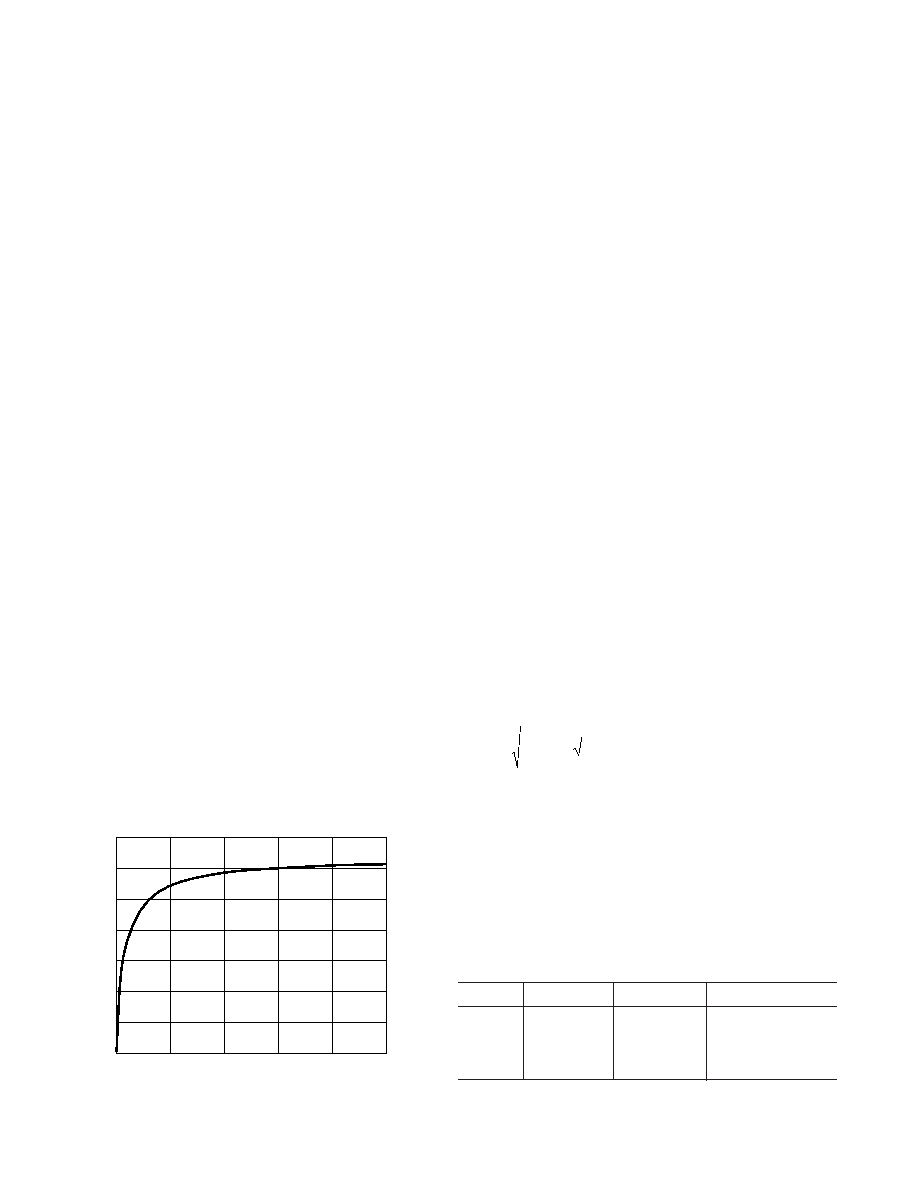
Varying the load impedance will result in 6 dB of additional gain
when RLOAD approaches infinity. The relationship between
RLOAD and gain is depicted in Figure 26 and is described by the
following equation:
Gain (dB) = [20 log ((2
RLOAD)/(RLOAD +75))]+(26–(0.7526
(71-Code)))
35
30
25
20
15
10
5
0
100
200
300
400
500
RLOAD –
Figure 26. Maximum Gain vs. RLOAD
GAIN
–
dB
Between Burst On/Off Transients, Asynchronous Power-
Down and DOCSIS
A 42% reduction in consumed power may be achieved asynchro
nously by applying Logic 0 to
PD Pin 6 activating the on-chip
“reverse amplifier.” The supply current is then reduced to
approximately 52 mA and the modem can no longer transmit in
the upstream direction. The on-chip reverse amplifier is designed
to reduce “between burst noise” and maintain a 75
W source
impedance to the low pass port of the modem’s diplexer while
minimizing power consumption. Changing the logic level applied
to the
PD pin will result in a Burst On/Off Transient at the
output of the AD8321. The transient results from switching
between the forward transmit amplifier and the powered down
(reverse) amplifier. Although the resulting transient meets the
DOCSIS transient amplitude requirements at maximum gain, it
is the lower gain range (i.e., 8 dBmV to 31 dBmV) where the
AD8321 may exceed the 7 mV maximum. The diplexer may
further reduce the glitch amplitude. An external RF switch, such
as Alpha Industries AS128-73 GaAs 2 Watt High Linearity
SPDT RF switch, may be used to further reduce the spurious
emissions, improve the isolation between the cable plant and the
upstream line driver and switch in a 75
W back termination
required to maintain proper line termination to the LP port of
the diplexer (see Figure 28).
Noise and DOCSIS
One of the most difficult issues facing designers of DOCSIS
compliant modems is maintaining a quiet output from the PA
during times when no information is being transmitted upstream.
In addition, maintaining proper signal-to-noise ratios serves to
ensure the quality of transmitted data. This is extremely critical
when the output signal of the modem is set to the minimum
DOCSIS specified output level or 8 dBmV. The AD8321 output
noise spectral density at minimum gain (or 8 dBmV) is 20 nV/
÷Hz
measured at 10 MHz. Considering the “Spurious Emissions
in 5 MHz to 42 MHz” of Table 4–8 in DOCSIS, the calculated
noise power in dBmV for 160 KSYM/SEC is:
2
20 log
20 nV / Hz 160E + 3 +60 or - 41 5
. dBmV
Comparing the computed noise power to the signal at 8 dBmV
yields –49.5 dBc or 3.5 dB higher than the required –53 dBc in
DOCSIS Table 4–8. An attenuator designed to match the
AD8321 75
W source to the 75 W load may be required. Refer
ring to the schematic of Figure 28 and the evaluation board
silkscreen of Figure 31, the matching attenuator is comprised of
the three resistors referred to as Rc, Rd and Re. Select the at
tenuation level from Table I such that noise floor is reduced to
levels specified in DOCSIS.
Table I.
Rc (
)
Rd (
)
Re (
)
Attenuation (dB)
1304
8.65
1304
–1
654.3
17.42
654.3
–2
432
26.1
432
–3
331.5
35.75
331.5
–4
–10–
REV. A
相关PDF资料 |
PDF描述 |
|---|---|
| MAX11614EEE+ | IC ADC SERIAL 12BIT 8CH 16-QSOP |
| MAX11210EEE+ | IC ADC 24BIT SPI/SRL 5SPS 16QSOP |
| MAX1111EEE+ | IC ADC 8BIT LP 16-QSOP |
| MAX1108EUB+ | IC ADC 8BIT LP 10-UMAX |
| MAX1110CAP+ | IC ADC SRL 8CH8BIT 50KSPS 20SSOP |
相关代理商/技术参数 |
参数描述 |
|---|---|
| AD8321ARZ-REEL2 | 制造商:AD 制造商全称:Analog Devices 功能描述:Gain Programmable CATV Line DRiver |
| AD8321-EVAL | 功能描述:BOARD EVAL FOR AD8321 RoHS:否 类别:编程器,开发系统 >> 评估演示板和套件 系列:- 产品培训模块:Obsolescence Mitigation Program 标准包装:1 系列:- 主要目的:电源管理,电池充电器 嵌入式:否 已用 IC / 零件:MAX8903A 主要属性:1 芯锂离子电池 次要属性:状态 LED 已供物品:板 |
| AD8321XR2 | 制造商:Analog Devices 功能描述: |
| AD8322 | 制造商:AD 制造商全称:Analog Devices 功能描述:5 V CATV Line Driver Coarse Step Output Power Control |
| AD8322ARU | 制造商:Analog Devices 功能描述:SP Amp Line Driver Amp Single 5.25V 28-Pin TSSOP Tube 制造商:Rochester Electronics LLC 功能描述:TSSOP COARSE STEP +5V CATV LINE DRIVER - Bulk |
发布紧急采购,3分钟左右您将得到回复。