- 您现在的位置:买卖IC网 > PDF目录373943 > AD8323-EVAL (Analog Devices, Inc.) 5 V CATV Line Driver Fine Step Output Power Control PDF资料下载
参数资料
| 型号: | AD8323-EVAL |
| 厂商: | Analog Devices, Inc. |
| 英文描述: | 5 V CATV Line Driver Fine Step Output Power Control |
| 中文描述: | 5伏精细有线电视线路驱动器输出功率控制步 |
| 文件页数: | 4/16页 |
| 文件大小: | 277K |
| 代理商: | AD8323-EVAL |
REV. 0
AD8323
–4–
ORDERING GUIDE
Model
Temperature Range
–40
°
C to +85
°
C
–40
°
C to +85
°
C
Package Description
JA
Package Option
AD8323ARU
AD8323ARU-REEL
AD8323-EVAL
28-Lead TSSOP
28-Lead TSSOP
Evaluation Board
67.7
°
C/W
*
67.7
°
C/W
*
RU-28
RU-28
*
Thermal Resistance measured on SEMI standard 4-layer board.
ABSOLUTE MAXIMUM RATINGS
*
Supply Voltage +V
S
Pins 5, 9, 10, 19, 20, 23, 27 . . . . . . . . . . . . . . . . . . . . . . 6 V
Input Voltages
Pins 25, 26 . . . . . . . . . . . . . . . . . . . . . . . . . . . . . . . .
±
0.5 V
Pins 1, 2, 3, 6, 7 . . . . . . . . . . . . . . . . . . . . . –0.8 V to +5.5 V
Internal Power Dissipation
TSSOP . . . . . . . . . . . . . . . . . . . . . . . . . . . . . . . . . . . 0.9 W
Operating Temperature Range . . . . . . . . . . . –40
°
C to +85
°
C
Storage Temperature Range . . . . . . . . . . . . –65
°
C to +150
°
C
Lead Temperature, Soldering 60 seconds . . . . . . . . . . . 300
°
C
*
Stresses above those listed under Absolute Maximum Ratings may cause perma-
nent damage to the device. This is a stress rating only; functional operation of the
device at these or any other conditions above those indicated in the operational
section of this specification is not implied. Exposure to absolute maximum rating
conditions for extended periods may affect device reliability.
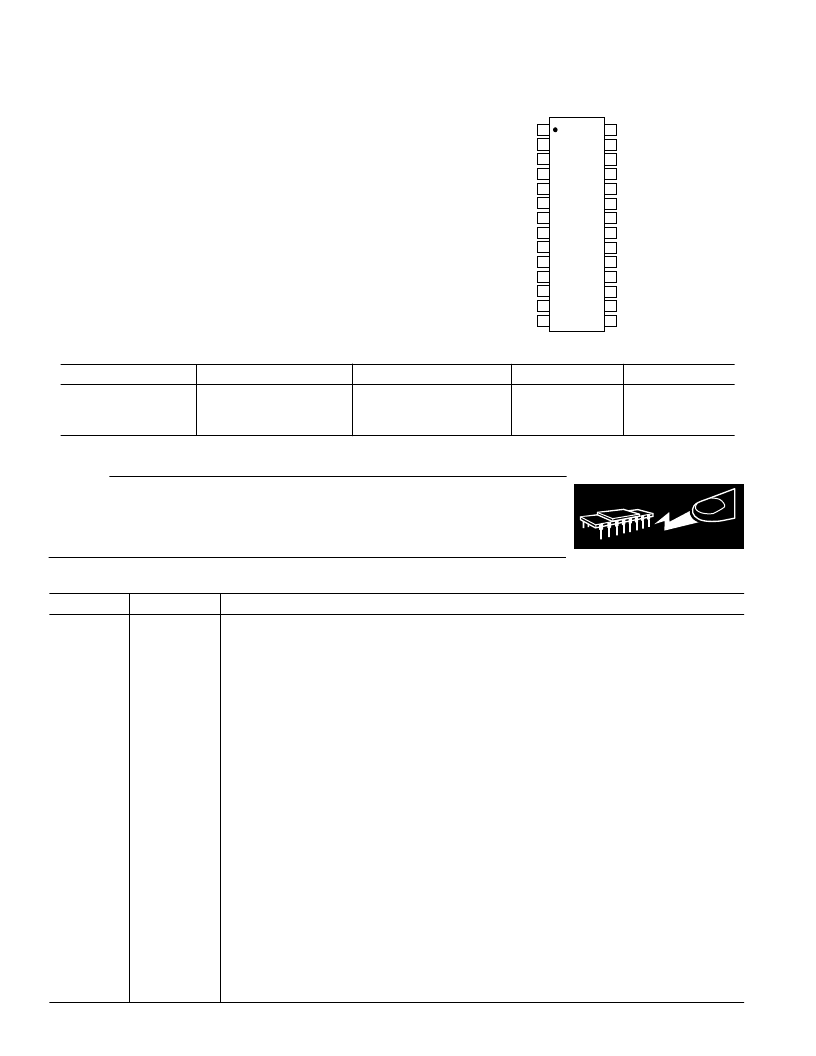
PIN CONFIGURATION
TOP VIEW
(Not to Scale)
28
27
26
25
24
23
22
21
20
19
18
17
16
15
1
2
3
4
5
6
7
8
9
10
11
12
13
14
AD8323
DATEN
GND
SDATA
V
CC
V
IN
–
V
IN+
GND
CLK
GND
V
CC
PD
V
CC
GND
SLEEP
GND
BYP
V
CC
V
CC
GND
V
CC
V
CC
GND
GND
GND
GND
GND
OUT
–
OUT+
CAUTION
ESD (electrostatic discharge) sensitive device. Electrostatic charges as high as 4000 V readily
accumulate on the human body and test equipment and can discharge without detection. Although
the AD8323 features proprietary ESD protection circuitry, permanent damage may occur on
devices subjected to high-energy electrostatic discharges. Therefore, proper ESD precautions are
recommended to avoid performance degradation or loss of functionality.
WARNING!
ESD SENSITIVE DEVICE
PIN FUNCTION DESCRIPTIONS
Pin No.
Mnemonic
Description
1
DATEN
Data Enable Low Input. This port controls the 8-bit parallel data latch and shift register. A Logic
0-to-1 transition transfers the latched data to the attenuator core (updates the gain) and simulta-
neously inhibits serial data transfer into the register. A 1-to-0 transition inhibits the data latch
(holds the previous gain state) and simultaneously enables the register for serial data load.
Serial Data Input. This digital input allows for an 8-bit serial (gain) word to be loaded into the
internal register with the MSB (Most Significant Bit) first.
Clock Input. The clock port controls the serial attenuator data transfer rate to the 8-bit master-
slave register. A Logic 0-to-1 transition latches the data bit and a 1-to-0 transfers the data bit to
the slave. This requires the input serial data word to be valid at or before this clock transition.
Common External Ground Reference.
2
SDATA
3
CLK
4, 8, 11,12,
13, 16, 17, 18,
22, 24, 28
5, 9, 10, 19,
20, 23, 27
6
7
GND
V
CC
Common Positive External Supply Voltage. A 0.1
μ
F capacitor must decouple each pin.
PD
SLEEP
Logic “0” powers down the part. Logic “1” powers up the part.
Low Power Sleep Mode. In the Sleep mode, the AD8323’s supply current is reduced to 4 mA. A
Logic “0” powers down the part (High Z
OUT
State) and a Logic “1” powers up the part.
Negative Output Signal.
Positive Output Signal.
Internal Bypass. This pin must be externally ac-coupled (0.1
μ
F cap).
Noninverting Input. DC-biased to approximately V
CC
/2. For single-ended inverting operation,
use a 0.1
μ
F decoupling capacitor and a 39.2
resistor between V
IN+
and ground.
Inverting Input. DC-biased to approximately V
CC
/2. Should be ac-coupled with a 0.1
μ
F capacitor.
14
15
21
25
OUT–
OUT+
BYP
V
IN+
26
V
IN–
相关PDF资料 |
PDF描述 |
|---|---|
| AD8325ARU | 5 V CATV Line Driver Fine Step Output Power Control |
| AD8325ARU-REEL | 5 V CATV Line Driver Fine Step Output Power Control |
| AD8325-EVAL | 5 V CATV Line Driver Fine Step Output Power Control |
| AD8325 | Fast Switching Digitally Controlled Variable Gain Amplifier(快速转换数字控制的可变增益放大器) |
| AD8326ARE-EVAL | ER 4C 4#0 PIN RECP |
相关代理商/技术参数 |
参数描述 |
|---|---|
| AD8324 | 制造商:AD 制造商全称:Analog Devices 功能描述:3.3 V Upstream Cable Line Driver |
| AD8324_05 | 制造商:AD 制造商全称:Analog Devices 功能描述:3.3 V Upstream Cable Line Driver |
| AD8324ACP | 制造商:Analog Devices 功能描述:SP Amp Line Driver Amp Single 3.47V 20-Pin LFCSP EP Tray 制造商:Rochester Electronics LLC 功能描述:+3.3 V UPSTREAM CABLE LINE DRIVER - Bulk |
| AD8324ACP-EVAL | 制造商:AD 制造商全称:Analog Devices 功能描述:3.3 V Upstream Cable Line Driver |
| AD8324ACP-R2 | 制造商:Analog Devices 功能描述:+3.3 V UPSTREAM CABLE LINE DRIVER - Tape and Reel |
发布紧急采购,3分钟左右您将得到回复。