- 您现在的位置:买卖IC网 > PDF目录373943 > AD8323-EVAL (Analog Devices, Inc.) 5 V CATV Line Driver Fine Step Output Power Control PDF资料下载
参数资料
| 型号: | AD8323-EVAL |
| 厂商: | Analog Devices, Inc. |
| 英文描述: | 5 V CATV Line Driver Fine Step Output Power Control |
| 中文描述: | 5伏精细有线电视线路驱动器输出功率控制步 |
| 文件页数: | 8/16页 |
| 文件大小: | 277K |
| 代理商: | AD8323-EVAL |
REV. 0
AD8323
–8–
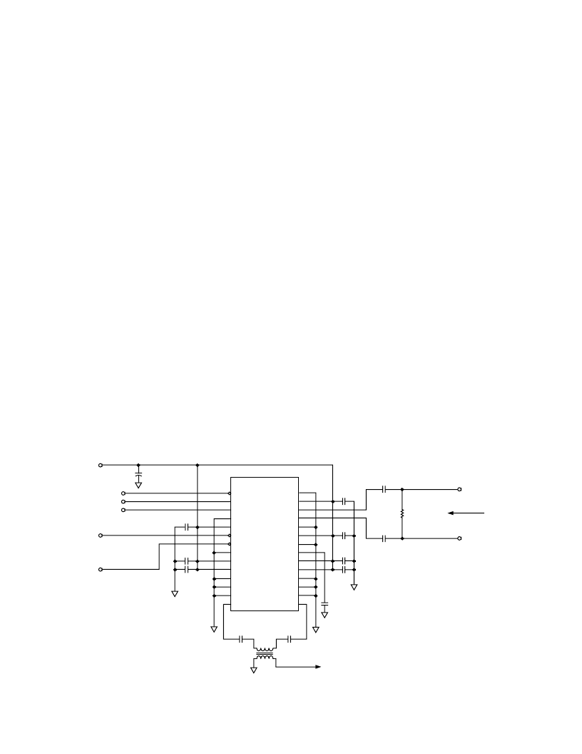
Output Bias, Impedance, and Termination
The differential output pins V
OUT+
and V
OUT
–
are also biased to
a dc level of approximately V
CC
/2. Therefore, the outputs should
be ac-coupled before being applied to the load. This may be
accomplished by connecting 0.1
μ
F capacitors in series with the
outputs as shown in the typical applications circuit of Figure 6.
The differential output impedance of the AD8323 is internally
maintained at 75
, regardless of whether the amplifier is in
forward transmit mode or reverse power-down mode, elimi-
nating the need for external back termination resistors. A 1:1
transformer (TOKO #617DB-A0070) is used to couple
the amplifier
’
s differential output to the coaxial cable while
maintaining a proper impedance match. If the output signal
is being evaluated on standard 50
test equipment, a 75
to
50
pad must be used to provide the test circuit with the
correct impedance match.
Power Supply Decoupling, Grounding, and Layout
Considerations
Careful attention to printed circuit board layout details will
prevent problems due to associated board parasitics. Proper RF
design technique is mandatory. The 5 V supply power should be
delivered to each of the V
CC
pins via a low impedance power bus
to ensure that each pin is at the same potential. The power bus
should be decoupled to ground with a 10
μ
F tantalum capacitor
located in close proximity to the AD8323. In addition to the
10
μ
F capacitor, each V
CC
pin should be individually decoupled to
ground with a 0.1
μ
F ceramic chip capacitor located as close to
the pin as possible. The pin labeled BYP (Pin 21) should also be
decoupled with a 0.1
μ
F capacitor. The PCB should have a low-
impedance ground plane covering all unused portions of the
component side of the board, except in the area of the input and
output traces (see Figure 11). It is important that all of the
AD8323
’
s ground pins are connected to the ground plane to
ensure proper grounding of all internal nodes. The differential
input and output traces should be kept as short and symmetrical
as possible. In addition, the input and output traces should be
kept far apart in order to minimize coupling (crosstalk) through
the board. Following these guidelines will improve the overall
performance of the AD8323 in all applications.
Initial Power-Up
When the 5 V supply is first applied to the V
CC
pins of the
AD8323, the gain setting of the amplifier is indeterminate.
Therefore, as power is first applied to the amplifier, the
PD
pin
should be held low (Logic 0) thus preventing forward signal
transmission. After power has been applied to the amplifier, the
gain can be set to the desired level by following the procedure in
the SPI Programming and Gain Adjustment section. The
PD
pin can then be brought from Logic 0 to 1, enabling forward
signal transmission at the desired gain level.
Asynchronous Power-Down
The asynchronous
PD
pin is used to place the AD8323 into
“
Between Burst
”
mode while maintaining a differential output
impedance of 75
. Applying a Logic 0 to the
PD
pin activates
the on-chip reverse amplifier, providing a 74% reduction in
consumed power. The supply current is reduced from approxi-
mately 133 mA to approximately 35 mA. In this mode of
operation, between burst noise is minimized and the amplifier
can no longer transmit in the upstream direction. In addition to
the
PD
pin, the AD8323 also incorporates an asynchronous
SLEEP
pin, which may be used to place the amplifier in a high
output impedance state and further reduce the supply current to
approximately 4 mA. Applying a Logic 0 to the
SLEEP
pin
places the amplifier into
SLEEP
mode. Transitioning into or
out of
SLEEP
mode will result in a transient voltage at the output
of the amplifier. Therefore, use only the
PD
pin for DOCSIS
compliant
“
Between Burst
”
operation.
DATEN
SDATA
CLK
GND1
V
CC
PD
SLEEP
GND2
V
CC1
V
CC2
GND3
GND4
GND5
OUT
–
GND11
V
CC6
V
IN
–
V
IN+
GND10
V
CC5
GND9
BYP
V
CC4
V
CC3
GND8
GND7
GND6
OUT+
AD8323TSSOP
5V
PD
SLEEP
DATEN
SDATA
CLK
10 F
25V
0.1 F
0.1 F
0.1 F
0.1 F
0.1 F
TOKO 617DB-A0070
TO DIPLEXER Z
IN
= 75
0.1 F
0.1 F
0.1 F
0.1 F
0.1 F
0.1 F
0.1 F
165
V
IN
–
V
IN+
Z
IN
= 150
Figure 6. Typical Applications Circuit
相关PDF资料 |
PDF描述 |
|---|---|
| AD8325ARU | 5 V CATV Line Driver Fine Step Output Power Control |
| AD8325ARU-REEL | 5 V CATV Line Driver Fine Step Output Power Control |
| AD8325-EVAL | 5 V CATV Line Driver Fine Step Output Power Control |
| AD8325 | Fast Switching Digitally Controlled Variable Gain Amplifier(快速转换数字控制的可变增益放大器) |
| AD8326ARE-EVAL | ER 4C 4#0 PIN RECP |
相关代理商/技术参数 |
参数描述 |
|---|---|
| AD8324 | 制造商:AD 制造商全称:Analog Devices 功能描述:3.3 V Upstream Cable Line Driver |
| AD8324_05 | 制造商:AD 制造商全称:Analog Devices 功能描述:3.3 V Upstream Cable Line Driver |
| AD8324ACP | 制造商:Analog Devices 功能描述:SP Amp Line Driver Amp Single 3.47V 20-Pin LFCSP EP Tray 制造商:Rochester Electronics LLC 功能描述:+3.3 V UPSTREAM CABLE LINE DRIVER - Bulk |
| AD8324ACP-EVAL | 制造商:AD 制造商全称:Analog Devices 功能描述:3.3 V Upstream Cable Line Driver |
| AD8324ACP-R2 | 制造商:Analog Devices 功能描述:+3.3 V UPSTREAM CABLE LINE DRIVER - Tape and Reel |
发布紧急采购,3分钟左右您将得到回复。