- 您现在的位置:买卖IC网 > PDF目录68990 > AD8339ACPZ (ANALOG DEVICES INC) 0 MHz - 50 MHz RF/MICROWAVE I/Q DEMODULATOR PDF资料下载
参数资料
| 型号: | AD8339ACPZ |
| 厂商: | ANALOG DEVICES INC |
| 元件分类: | 调制器/解调器 |
| 英文描述: | 0 MHz - 50 MHz RF/MICROWAVE I/Q DEMODULATOR |
| 封装: | 6 X 6 MM, ROHS COMPLIANT, MO-220-VJJD-2, LFCSP-40 |
| 文件页数: | 11/36页 |
| 文件大小: | 2970K |
| 代理商: | AD8339ACPZ |
第1页第2页第3页第4页第5页第6页第7页第8页第9页第10页当前第11页第12页第13页第14页第15页第16页第17页第18页第19页第20页第21页第22页第23页第24页第25页第26页第27页第28页第29页第30页第31页第32页第33页第34页第35页第36页
AD8339
Rev. A | Page 19 of
36
QUADRATURE GENERATION
The internal 0° and 90° LO phases are digitally generated by a
divide-by-4 logic circuit. The divider is dc-coupled and inherently
broadband; the maximum LO frequency is limited only by its
switching speed. The duty cycle of the quadrature LO signals
is intrinsically 50% and is unaffected by the asymmetry of the
externally connected 4LO input. Furthermore, the divider is
implemented such that the 4LO signal reclocks the final flip-
flops that generate the internal LO signals and thereby minimizes
noise introduced by the divide circuitry.
For optimum performance, the 4LO input is driven differentially,
but it can also be driven single-ended. A good choice for a drive
is an LVDS device as is done on the AD8339 evaluation board.
The common-mode range on each pin is approximately 0.2 V to
3.8 V with the nominal ±5 V supplies.
The minimum 4LO level is frequency dependent when driven
by a sine wave. For optimum noise performance, it is important
to ensure that the LO source has very low phase noise (jitter)
and adequate input level to ensure stable mixer core switching.
The gain through the divider determines the LO signal level vs.
RF frequency. The AD8339 can be operated at very low frequen-
cies at the LO inputs if a square wave is used to drive the LO, as
is done with the LVDS driver on the evaluation board.
Beamforming applications require a precise channel-to-channel
phase relationship for coherence among multiple channels. A
reset pin is provided to synchronize the LO divider circuits in
different AD8339s when they are used in arrays. The RSET pin
resets the dividers to a known state after power is applied to
multiple AD8339s. A logic input must be provided to the RSET
pin when using more than one AD8339. Note that at least one
channel must be enabled for the LO interface to also be enabled
and the LO reset to work. See the Reset Input section for more
information.
I/Q DEMODULATOR AND PHASE SHIFTER
The I/Q demodulators consist of double-balanced Gilbert cell
mixers. The RF input signals are converted into currents by
transconductance stages that have a maximum differential input
signal capability of 2.8 V p-p. These currents are then presented
to the mixers, which convert them to baseband (RF LO) and
twice RF (RF + LO). The signals are phase shifted according to
the codes programmed into the SPI latch (see Table 4); the
phase bits are labeled PHx0 through PHx3, where 0 indicates
LSB and 3 indicates MSB. The phase shift function is an integral
part of the overall circuit. The phase shift
listed in Column 1 of
Table 4 is defined as being between the
baseband I or Q channel
outputs. As an example, for a common
signal applied to a pair of
RF inputs to an AD8339, the baseband
outputs are in phase for
matching phase codes. However, if the
phase code for Channel 1
is 0000 and that of Channel 2 is 0001,
then Channel 2 leads
Channel 1 by 22.5°.
Following the phase shift circuitry, the differential current
signal is converted from differential to single-ended via a
current mirror. An external transimpedance amplifier is needed
to convert the I and Q outputs to voltages.
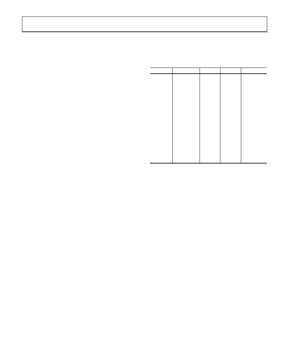
Table 4. Phase Select Code for Channel-to-Channel Phase Shift
Φ Shift
PHx3 (MSB)
PHx2
PHx1
PHx0 (LSB)
0°
0
22.5°
0
1
45°
0
1
0
67.5°
0
1
90°
0
1
0
112.5°
0
1
0
1
135°
0
1
0
157.5°
0
1
180°
1
0
202.5°
1
0
1
225°
1
0
1
0
247.5°
1
0
1
270°
1
0
292.5°
1
0
1
315°
1
0
337.5°
1
DYNAMIC RANGE AND NOISE
Figure 53 is an interconnection block diagram of all four channels
of the AD8339. More channels are easily added to the summation
(up to 16 when using an AD8021 as the summation amplifier)
by wire-OR connecting the outputs as shown for four channels.
For optimum system noise performance, the RF input signal is
provided by a very low noise amplifier, such as the LNA of the
the I and Q outputs of a number of receiver channels are summed
(for example, the four channels illustrated in Figure 53). The
dynamic range of the system increases by the factor 10 log10(N),
where N is the number of channels (assuming random uncorre-
lated noise). The noise in the 4-channel example of Figure 53 is
increased by 6 dB while the signal quadruples (12 dB), yielding
an aggregate SNR improvement of 6 dB (12 6).
Judicious selection of the RF amplifier ensures the least degrada-
tion in dynamic range. The input referred spectral voltage noise
density (en) of the AD8339 is nominally ~11 nV/√Hz. For the
noise of the AD8339 to degrade the system noise figure (NF) by
1 dB, the combined noise of the source and the LNA should be
approximately twice that of the AD8339, or 22 nV/√Hz. If the
noise of the circuitry before the AD8339 is less than 22 nV/√Hz,
the system NF degrades more than 1 dB. For example, if the
noise contribution of the LNA and source is equal to the AD8339,
or 11 nV/√Hz, the degradation is 3 dB. If the circuit noise
preceding the AD8339 is 1.3× as large as that of the AD8339 (or
~14 nV/√Hz), the degradation is 2 dB. For a circuit noise 1.45×
that of the AD8339 (16 nV/√Hz), the degradation is 1.5 dB.
相关PDF资料 |
PDF描述 |
|---|---|
| ADL5374ACPZ-WP | 3000 MHz - 4000 MHz RF/MICROWAVE QUADRAPHASE MODULATOR |
| ADL5375-05ACPZ-R7 | 400 MHz - 6000 MHz RF/MICROWAVE I/Q MODULATOR |
| AH212-S8G | 1800 MHz - 2400 MHz RF/MICROWAVE NARROW BAND MEDIUM POWER AMPLIFIER |
| AK1222 | 100 MHz - 900 MHz RF/MICROWAVE SINGLE BALANCED MIXER |
| ALM-40220-BLKG | 2010 MHz - 2025 MHz RF/MICROWAVE SGL POLE DOUBLE THROW SWITCH, 0.45 dB INSERTION LOSS |
相关代理商/技术参数 |
参数描述 |
|---|---|
| AD8339ACPZ-R7 | 功能描述:IC DEMODULATOR I/Q QUAD 40LFCSP RoHS:是 类别:RF/IF 和 RFID >> RF 解调器 系列:- 产品培训模块:Lead (SnPb) Finish for COTS Obsolescence Mitigation Program 标准包装:2,500 系列:- 功能:解调器 LO 频率:- RF 频率:70MHz ~ 300MHz P1dB:-9dBm 增益:- 噪音数据:6.36dB 电流 - 电源:41.5mA 电源电压:2.7 V 封装/外壳:28-WFQFN 裸露焊盘 供应商设备封装:28-TQFN-EP(5x5) 包装:带卷 (TR) |
| AD8339ACPZ-RL | 功能描述:IC DEMODULATOR I/Q QUAD 40LFCSP RoHS:是 类别:RF/IF 和 RFID >> RF 解调器 系列:- 产品培训模块:Lead (SnPb) Finish for COTS Obsolescence Mitigation Program 标准包装:2,500 系列:- 功能:解调器 LO 频率:- RF 频率:70MHz ~ 300MHz P1dB:-9dBm 增益:- 噪音数据:6.36dB 电流 - 电源:41.5mA 电源电压:2.7 V 封装/外壳:28-WFQFN 裸露焊盘 供应商设备封装:28-TQFN-EP(5x5) 包装:带卷 (TR) |
| AD8339-EVALZ | 功能描述:BOARD EVAL AD8339 I/Q DEMOD RoHS:是 类别:RF/IF 和 RFID >> RF 评估和开发套件,板 系列:- 标准包装:1 系列:- 类型:GPS 接收器 频率:1575MHz 适用于相关产品:- 已供物品:模块 其它名称:SER3796 |
| AD834 | 制造商:AD 制造商全称:Analog Devices 功能描述:500 MHz Four-Quadrant Multiplier |
| AD834_12 | 制造商:AD 制造商全称:Analog Devices 功能描述:500 MHz Four-Quadrant Multiplier |
发布紧急采购,3分钟左右您将得到回复。