- 您现在的位置:买卖IC网 > PDF目录373944 > AD8346-EVAL (Analog Devices, Inc.) 0.8 GHz-2.5 GHz Quadrature Modulator PDF资料下载
参数资料
| 型号: | AD8346-EVAL |
| 厂商: | Analog Devices, Inc. |
| 英文描述: | 0.8 GHz-2.5 GHz Quadrature Modulator |
| 中文描述: | 0.8千兆赫,2.5 GHz的正交调制器 |
| 文件页数: | 4/12页 |
| 文件大小: | 190K |
| 代理商: | AD8346-EVAL |
REV. 0
AD8346
–4–
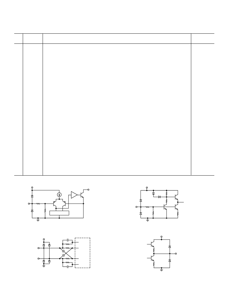
PIN FUNCTION DESCRIPTIONS
Equivalent
Circuit
Pin
Name
Description
1
IBBP
I Channel Baseband Positive Input Pin. Input should be dc biased to approximately 1.2 V.
Nominal characterized ac swing is 1 V p-p (0.7 V to 1.7 V). This makes the differential
input 2 V p-p when IBBN is 180 degrees out of phase from IBBP.
I Channel Baseband Negative Input Pin. Input should be dc biased to approximately 1.2 V.
Nominal characterized ac swing is 1 V p-p (0.7 V to 1.7 V). This makes the differential
input 2 V p-p when IBBN is 180 degrees out of phase from IBBP.
Ground pin for the LO phase splitter and LO buffers.
Ground pin for the LO phase splitter and LO buffers.
LO Negative Input Pin. Internal dc bias (approximately VPS1–800 mV) is supplied. This
pin must be ac coupled.
LO Positive Input Pin. Internal dc bias (approximately VPS1–800 mV) is supplied. This
pin must be ac coupled.
Power supply pin for the bias cell and LO buffers. This pin should be decoupled using
local 100 pF and 0.01
μ
F capacitors.
Enable Pin. A high level enables the device; a low level puts the device in sleep mode.
Ground pin for the input stage of output amplifier.
Ground pin for the output stage of output amplifier.
50
DC Coupled RF Output. User must provide ac coupling on this pin.
Power supply pin for Baseband input voltage to current converters and mixer core. This pin
should be decoupled using local 100 pF and 0.01
μ
F capacitors.
Ground pin for Baseband input voltage to current converters and mixer core.
Ground pin for Baseband input voltage to current converters and mixer core.
Q Channel Baseband Negative Input. Input should be dc biased to approximately 1.2 V.
Nominal characterized ac swing is 1 V p-p. This makes the differential input 2 V p-p when
QBBN is 180 degrees out of phase from QBBP.
Q Channel Baseband Positive Input. Input should be dc biased to approximately 1.2 V.
Nominal characterized ac swing is 1 V p-p. This makes the differential input 2 V p-p when
QBBN is 180 degrees out of phase from QBBP.
Circuit A
2
IBBN
Circuit A
3
4
5
COM1
COM1
LOIN
Circuit B
6
LOIP
Circuit B
7
VPS1
8
9
10
11
12
ENBL
COM2
COM3
VOUT
VPS2
Circuit C
Circuit D
13
14
15
COM4
COM4
QBBN
Circuit A
16
QBBP
Circuit A
3k
V
9k
V
VPS2
INPUT
BUFFER
TO MIXER
CORE
ACTIVE LOADS
Circuit A
VPS1
LOIN
LOIP
PHASE
SPLITTER
CONTINUES
Circuit B
40k
V
30k
V
VPS1
TO BIAS FOR
STARTUP/
SHUTDOWN
780
V
75k
V
ENBL
75k
V
Circuit C
43
V
43
V
VPS2
V
OUT
Circuit D
Figure 1. Equivalent Circuits
相关PDF资料 |
PDF描述 |
|---|---|
| AD8346ARU | 0.8 GHz-2.5 GHz Quadrature Modulator |
| AD8346ARU-REEL7 | 0.8 GHz-2.5 GHz Quadrature Modulator |
| AD8347ARU-REEL | 0.8 GHz-2.7 GHz Direct Conversion Quadrature Demodulator |
| AD8347 | 0.8 GHz-2.7 GHz Direct Conversion Quadrature Demodulator |
| AD8347-EVAL | 0.8 GHz-2.7 GHz Direct Conversion Quadrature Demodulator |
相关代理商/技术参数 |
参数描述 |
|---|---|
| AD8346-EVALZ | 制造商:Analog Devices 功能描述:- Bulk |
| AD8347 | 制造商:AD 制造商全称:Analog Devices 功能描述:0.8 GHz-2.7 GHz Direct Conversion Quadrature Demodulator |
| AD8347ARU | 功能描述:IC QUADRATURE DEMOD 28-TSSOP RoHS:否 类别:RF/IF 和 RFID >> RF 解调器 系列:- 产品培训模块:Lead (SnPb) Finish for COTS Obsolescence Mitigation Program 标准包装:2,500 系列:- 功能:解调器 LO 频率:- RF 频率:70MHz ~ 300MHz P1dB:-9dBm 增益:- 噪音数据:6.36dB 电流 - 电源:41.5mA 电源电压:2.7 V 封装/外壳:28-WFQFN 裸露焊盘 供应商设备封装:28-TQFN-EP(5x5) 包装:带卷 (TR) |
发布紧急采购,3分钟左右您将得到回复。