- 您现在的位置:买卖IC网 > PDF目录373944 > AD8347ARU-REEL7 (ANALOG DEVICES INC) 0.8 GHz-2.7 GHz Direct Conversion Quadrature Demodulator PDF资料下载
参数资料
| 型号: | AD8347ARU-REEL7 |
| 厂商: | ANALOG DEVICES INC |
| 元件分类: | 衰减器 |
| 英文描述: | 0.8 GHz-2.7 GHz Direct Conversion Quadrature Demodulator |
| 中文描述: | 800 MHz - 2700 MHz RF/MICROWAVE QUADRAPHASE DEMODULATOR |
| 封装: | MO-153AE, RU-28, TSSOP-28 |
| 文件页数: | 14/20页 |
| 文件大小: | 750K |
| 代理商: | AD8347ARU-REEL7 |
REV. 0
AD8347
–14–
less than
400
μ
A of supply current. The reference voltage (VREF)
of 1.0 V,
which serves as the common-mode reference for the
baseband circuits, is made available for external use.
OPERATING THE AD8347
Basic Connections
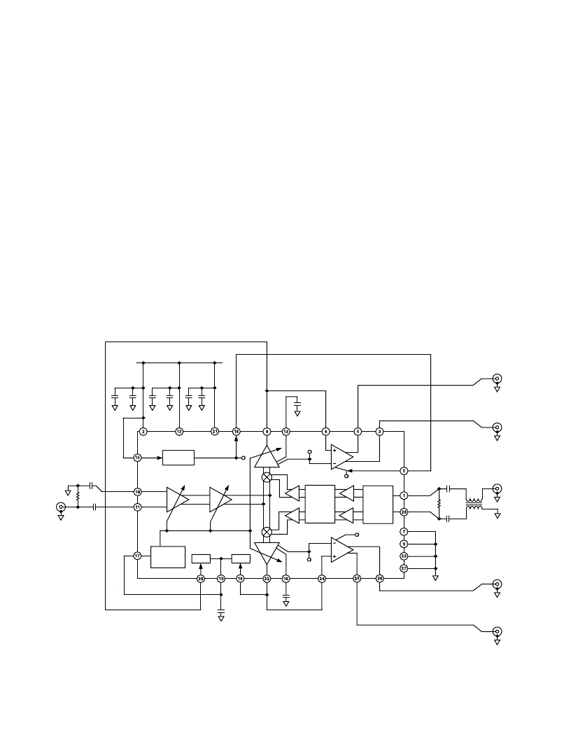
Figure 4 shows the basic connections for operating the AD8347.
The device is powered through three power supply pins: VPS1,
VPS2, and VPS3. These pins supply current to different parts of
the overall circuit. VPS1 and VPS2 power the Local Oscillator (LO)
and RF sections, respectively, while VPS3 powers the baseband
amplifiers. While all of these pins should be connected to the same
supply voltage, each pin should be separately decoupled
using two
capacitors. 100 pF and 0.1
μ
F are recommended (values close
to these may also be used).
A supply voltage in the range 2.7 V to 5.5 V should be used. The
quiescent current is 64 mA when operating from a 5 V supply.
By pulling the ENBL pin low, the device goes into its power- down
mode. The power-down current is 400
μ
A when operating on a
5 V supply and 80
μ
A on a 2.7 V supply.
Like the supply pins, the individual sections of the circuit are
separately grounded. COM1, COM2, and COM3 provide ground
for the LO, RF, and baseband sections respectively. All of these
pins should be connected to the same low impedance ground.
RF Input and Matching
The RF input signal should be ac-coupled into the RFIP pin and
RFIN should be ac-coupled to ground. To improve broadband
matching to a 50
source, a 200
resistor may be connected
from the signal side of RFIP’s coupling capacitor to ground.
LO Drive Interface
For optimum performance the LO inputs, LOIN and LOIP,
should be driven differentially. M/A-COM balun, ETC1-1-13
is recommended. Unless an (ac-coupled) transformer is being
used to generate the differential LO, the inputs must be ac-coupled
as shown. To improve broadband matching to a 50
source, a
200
shunt resistor may be connected between LOIP and LOIN.
An LO drive level of –8 dBm is recommended. TPC 17a shows
the relationship between LO drive level, LO frequency, and
quadrature error for a typical device.
A single-ended drive is also possible as shown in Figure 5, but
this will slightly increase LO leakage. The LO signal should be
applied through a coupling capacitor to LOIP, and LOIN should
be ac-coupled to ground. Because the inputs are fully differen-
tial, the drive orientation can be reversed. As in the case of the
differential drive, a 200
resistor connected across LOIP and
LOIN improves the match to a 50
source.
RFIN
VREF
RFIP
VPS2
IMXO
COM3
IOPP
IOFS
IOPN
VCMO
VPS1
LOIN
IAIN
COM2
QOPN
COM3
VGIN
ENBL
LOIP
COM1
VPS3
AD8347
PHASE
SPLITTER
1
BIAS
CELL
DET 1
VREF
VREF
GAIN
CONTROL
INTERFACE
DET 2
VREF
VCMO
PHASE
SPLITTER
2
VCMO
VDT2
QMXO
QOPP
QOFS
C14
0.1 F
VAGC
VDT1
QAIN
760mV p-p
DIFFERENTIAL
(AGC MODE)
V
CM
= 1V
QOPP
QOPN
LO INPUT
–
8dBm
0.8GHz
–
2.7GHz
T1
ETC 1-1-13
(M/A-COM)
1
5
3
4
C4
100pF
R17
200
C3
100pF
760mV p-p
DIFFERENTIAL
(AGC MODE)
V
CM
= 1V
C10
100pF
C9
0.1 F
C8
100pF
C7
0.1 F
C6
0.1 F
C5
100pF
+V
S
(2.7V
–
5.5V)
RF INPUT
0.8GHz
–
2.7GHz
0dBm MAX
(AGC MODE)
C1
100pF
C2
100pF
R1
200
24mV p-p
(AGC MODE)
1V BIAS (VREF)
24mV p-p
(AGC MODE)
1V BIAS (VREF)
C13
0.1 F
IOPP
IOPN
C15
0.1 F
Figure 4. Basic Connections
相关PDF资料 |
PDF描述 |
|---|---|
| AD8348 | 50-1000 MHz Quadrature Demodulator |
| AD8348-EVAL | 50-1000 MHz Quadrature Demodulator |
| AD8348XXX | 50-1000 MHz Quadrature Demodulator |
| AD8349 | 700 MHz to 2700 MHz Quadrature Modulator |
| AD8349ARE | 700 MHz to 2700 MHz Quadrature Modulator |
相关代理商/技术参数 |
参数描述 |
|---|---|
| AD8347ARUZ | 功能描述:IC QUADRATURE DEMOD 28-TSSOP RoHS:是 类别:RF/IF 和 RFID >> RF 解调器 系列:- 产品培训模块:Lead (SnPb) Finish for COTS Obsolescence Mitigation Program 标准包装:2,500 系列:- 功能:解调器 LO 频率:- RF 频率:70MHz ~ 300MHz P1dB:-9dBm 增益:- 噪音数据:6.36dB 电流 - 电源:41.5mA 电源电压:2.7 V 封装/外壳:28-WFQFN 裸露焊盘 供应商设备封装:28-TQFN-EP(5x5) 包装:带卷 (TR) |
| AD8347ARUZ | 制造商:Analog Devices 功能描述:IC QUAD DEMODULATOR 0.8-2.7GHZ 28-TSSOP |
| AD8347ARUZ-REEL7 | 功能描述:IC QUADRATURE DEMOD 28-TSSOP TR RoHS:是 类别:RF/IF 和 RFID >> RF 解调器 系列:- 产品培训模块:Lead (SnPb) Finish for COTS Obsolescence Mitigation Program 标准包装:2,500 系列:- 功能:解调器 LO 频率:- RF 频率:70MHz ~ 300MHz P1dB:-9dBm 增益:- 噪音数据:6.36dB 电流 - 电源:41.5mA 电源电压:2.7 V 封装/外壳:28-WFQFN 裸露焊盘 供应商设备封装:28-TQFN-EP(5x5) 包装:带卷 (TR) |
| AD8347-EVAL | 制造商:Analog Devices 功能描述:EVALUATION BOARD ((NS)) |
| ad8347-evalz | 制造商:Analog Devices 功能描述:EVAL BD 0.8 GHZ TO 2.7 GHZ DIRECT CONVERSION QUADRATURE DEMO - Bulk |
发布紧急采购,3分钟左右您将得到回复。