- 您现在的位置:买卖IC网 > PDF目录373944 > AD8347ARU-REEL7 (ANALOG DEVICES INC) 0.8 GHz-2.7 GHz Direct Conversion Quadrature Demodulator PDF资料下载
参数资料
| 型号: | AD8347ARU-REEL7 |
| 厂商: | ANALOG DEVICES INC |
| 元件分类: | 衰减器 |
| 英文描述: | 0.8 GHz-2.7 GHz Direct Conversion Quadrature Demodulator |
| 中文描述: | 800 MHz - 2700 MHz RF/MICROWAVE QUADRAPHASE DEMODULATOR |
| 封装: | MO-153AE, RU-28, TSSOP-28 |
| 文件页数: | 16/20页 |
| 文件大小: | 750K |
| 代理商: | AD8347ARU-REEL7 |
REV. 0
AD8347
–16–
approximately 24 mV p-p. If this signal is applied directly to the
subsequent baseband amplifier stage, the final baseband output
is 760 mV p-p differential. (See Baseband Amplifier section.)
If the VGA gain is being set from an external source, the on-board
detector inputs (VDT1 and VDT2) are not used and should be
tied to VREF.
Note that in subsequent sections, peak-to-peak calculations
assume a sine wave input. If the input signal has a higher peak-
to-average ratio, the mixer output peak-to-peak voltage at which
the AGC loop settles will be higher.
Changing the AGC Setpoint
The AGC circuit can be easily set up to level at voltages higher
than the nominal 24 mV p-p as shown in Figure 6. The voltages
on Pins IMXO and QMXO are attenuated before being applied
to the detector inputs. In the example shown, an attenuation
factor of 0.2 (–14 dB) between IMXO/QMXO and the detector
inputs, will cause the VGA to level at approximately 120 mV p-p
(note that resistor divider network must be referenced to V
VREF
).
This results in a peak-to-peak output swing at the baseband
amplifier outputs of 3.8 V differential, that is, 1.6 V to 3.4 V on
each side. Note that V
VCMO
has been increased to 2.5 V to avoid
signal clipping at the baseband outputs. Due to the attenuation
between the mixer output and the detector input, the variation
in the settled mixer output level, versus RF input power, will be
greater than the variation shown in TPC 30. The variation will
be greater by a factor equal to the inverse of the attenuation factor.
Baseband Amplifiers
The final baseband amplifier stage takes the signals from IMXO/
QMXO and amplifies them by 30 dB, or a factor of 31.6. This
results in a maximum system gain of 69.5 dB. When the VGA is
in AGC mode, the baseband I & Q outputs (IOPN, IOPP,
QOPN, and QOPP) deliver a differential voltage of approxi-
mately 760 mV p-p (380 mV p-p on each side).
The single-ended input signal to the baseband amplifiers is
applied at the high impedance inputs IAIN and QAIN. As can
be seen in Figure 4, the baseband amplifier operates internally
as a differential amplifier, with the second input being driven by
V
VREF
. As a result, the input signal to the baseband amplifier
should be biased at V
VREF
.
The output common-mode level of the baseband amplifiers is
set by the voltage on Pin 5, VCMO. This pin can either be
connected to VREF (Pin 14) or to an external reference voltage
from a device such as an analog-to-digital converter (ADC).
V
VCMO
has a nominal range from 0.5 V to 2.5 V. However, since
the baseband amplifiers can only swing down to 0.4 V, higher
values of V
VCMO
will generally be required to avoid low-end
signal clipping. On the other hand, the positive swing at each
output is limited to 1.3 V below the supply voltage. So the max
p-p swing is given by 2 (V
PS
– 1.3 – 0.4) V differentially.
For example, in order for the baseband output amplifier to be able
to deliver an output swing of 2 V p-p (1 V p-p on each side),
V
VCMO
must be in the range from 0.9 V to 2.5 V.
The differential output offset voltages of the baseband amplifiers
are typically
±
50 mV. This offset voltage results from both input
and output effects.
The overall signal-to-noise ratio can be improved by increasing
the VGA gain by driving it with an external voltage or by changing
the setpoint of the AGC circuit. (See Changing the AGC Setpoint.)
Driving Capacitive Loads
In applications where the baseband amplifiers are driving unbal-
anced capacitive loads, some series resistance should be placed
between the amplifier and the capacitive load. For example, for
a 10 pF load, four 220
series resistors (one in each baseband
output) should be used.
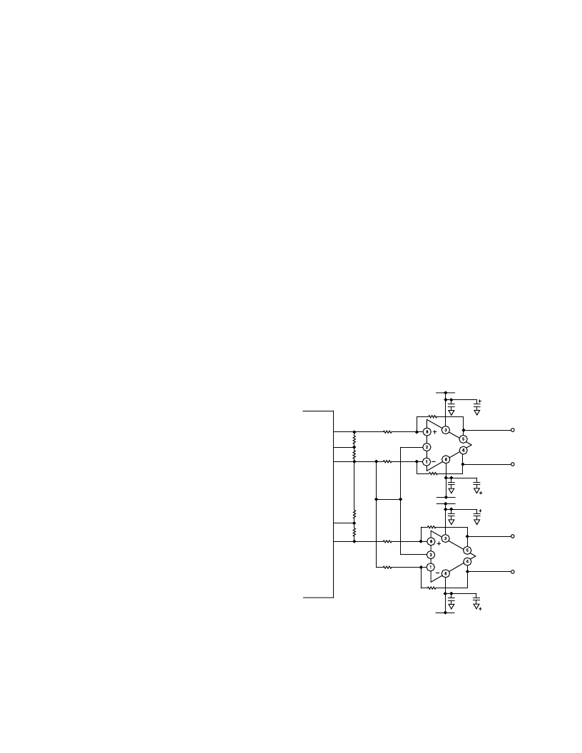
External Baseband Amplification
The baseband output offset voltage and noise can be reduced by
bypassing the internal baseband amplifiers and amplifying the
mixer output signal using a high quality differential amplifier. In
the example shown in Figure 7, two AD8132 differential ampli-
fiers are used to gain the mixer output signals up by 20 dB. In this
example, the setpoint of the AGC circuit has been increased so that
the input to the external amplifiers is approximately 72 mV p-p.
This results in final baseband output signals of 720 mV p-p.
The closed-loop bandwidth of the amplifiers in Figure 7 is equal
to roughly 20 MHz. Higher bandwidths are achievable, but at
the cost of lower closed-loop gain. In Figure 7, the output common
mode levels (VOCM, Pin 2) of the differential amplifiers are set
by the AD8347’s VREF (approximately 1 V). The output common
mode levels can also be set externally (e.g., by the reference voltage
from an ADC).
IMXO
AD8347
VREF
10 F
0.1 F
QMXO
VDT1
720mV p-p
DIFFERENTIAL
V
CM
= 1V
R19A
4.99k
+5V
10 F
0.1 F
AD8132
R17A
499
R18A
499
R22
20k
R23
10k
72mV p-p
VDT2
72mV p-p
R25
20k
R24
10k
R17B
499
4.99k
R20A
4.99k
R19B
+5V
–
5V
R18B
499
720mV p-p
DIFFERENTIAL
V
CM
= 1V
–
5V
4.99k
R20B
10 F
0.1 F
10 F
0.1 F
AD8132
Figure 7. External Baseband Amplification Example
相关PDF资料 |
PDF描述 |
|---|---|
| AD8348 | 50-1000 MHz Quadrature Demodulator |
| AD8348-EVAL | 50-1000 MHz Quadrature Demodulator |
| AD8348XXX | 50-1000 MHz Quadrature Demodulator |
| AD8349 | 700 MHz to 2700 MHz Quadrature Modulator |
| AD8349ARE | 700 MHz to 2700 MHz Quadrature Modulator |
相关代理商/技术参数 |
参数描述 |
|---|---|
| AD8347ARUZ | 功能描述:IC QUADRATURE DEMOD 28-TSSOP RoHS:是 类别:RF/IF 和 RFID >> RF 解调器 系列:- 产品培训模块:Lead (SnPb) Finish for COTS Obsolescence Mitigation Program 标准包装:2,500 系列:- 功能:解调器 LO 频率:- RF 频率:70MHz ~ 300MHz P1dB:-9dBm 增益:- 噪音数据:6.36dB 电流 - 电源:41.5mA 电源电压:2.7 V 封装/外壳:28-WFQFN 裸露焊盘 供应商设备封装:28-TQFN-EP(5x5) 包装:带卷 (TR) |
| AD8347ARUZ | 制造商:Analog Devices 功能描述:IC QUAD DEMODULATOR 0.8-2.7GHZ 28-TSSOP |
| AD8347ARUZ-REEL7 | 功能描述:IC QUADRATURE DEMOD 28-TSSOP TR RoHS:是 类别:RF/IF 和 RFID >> RF 解调器 系列:- 产品培训模块:Lead (SnPb) Finish for COTS Obsolescence Mitigation Program 标准包装:2,500 系列:- 功能:解调器 LO 频率:- RF 频率:70MHz ~ 300MHz P1dB:-9dBm 增益:- 噪音数据:6.36dB 电流 - 电源:41.5mA 电源电压:2.7 V 封装/外壳:28-WFQFN 裸露焊盘 供应商设备封装:28-TQFN-EP(5x5) 包装:带卷 (TR) |
| AD8347-EVAL | 制造商:Analog Devices 功能描述:EVALUATION BOARD ((NS)) |
| ad8347-evalz | 制造商:Analog Devices 功能描述:EVAL BD 0.8 GHZ TO 2.7 GHZ DIRECT CONVERSION QUADRATURE DEMO - Bulk |
发布紧急采购,3分钟左右您将得到回复。