- 您现在的位置:买卖IC网 > PDF目录97841 > AD8347ARUZ-REEL7 (ANALOG DEVICES INC) 800 MHz - 2700 MHz RF/MICROWAVE QUADRAPHASE DEMODULATOR PDF资料下载
参数资料
| 型号: | AD8347ARUZ-REEL7 |
| 厂商: | ANALOG DEVICES INC |
| 元件分类: | 调制器/解调器 |
| 英文描述: | 800 MHz - 2700 MHz RF/MICROWAVE QUADRAPHASE DEMODULATOR |
| 封装: | MO-153AE, RU-28, TSSOP-28 |
| 文件页数: | 13/28页 |
| 文件大小: | 623K |
| 代理商: | AD8347ARUZ-REEL7 |
第1页第2页第3页第4页第5页第6页第7页第8页第9页第10页第11页第12页当前第13页第14页第15页第16页第17页第18页第19页第20页第21页第22页第23页第24页第25页第26页第27页第28页
AD8347
Rev. A | Page 20 of 28
RFIN
VREF
RFIP
VPS2
IMXO
COM3
IOPP
IOFS
IOPN
VCMO
VPS1
LOIN
IAIN
COM2
QOPN
COM3
ENBL
LOIP
COM1
VPS3
AD8347
PHASE
SPLITTER
1
BIAS
CELL
DET 1
VREF
GAIN
CONTROL
INTERFACE
DET 2
VREF
VCMO
PHASE
SPLITTER
2
VCMO
VDT2
QMXO
QOPP
QOFS
VAGC
VDT1
QAIN
QOPP
QOPN
LO INPUT
–8dBm
0.8GHz–2.7GHz
T1
ETC 1-1-13
(M/A-COM)
15
3
4
C4
100pF
R17
200
Ω
C3
100pF
3.8V p-p
DIFFERENTIAL
VCM = 2.5V
C10
100pF
C9
0.1
μF
C8
100pF
C7
0.1
μF
C6
0.1
μF
C5
100pF
RF
INPUT
C2
100pF
C1
100pF
R1
200
Ω
C14
0.1
μF
120mV p-p
1V BIAS
120mV p-p
1V BIAS
C13
0.1
μF
IOPP
IOPN
R20
4k
Ω
R19
1k
Ω
2.5V
3.8V p-p
DIFFERENTIAL
VCM = 2.5V
R21
4k
Ω
R22
1k
Ω
+VS +5V
02675-048
4
6
13
8
14
21
12
2
15
10
11
17
20
19
18
22
16
24
25
26
27
23
9
7
1
28
5
3
C16
0.1
μF
VGIN
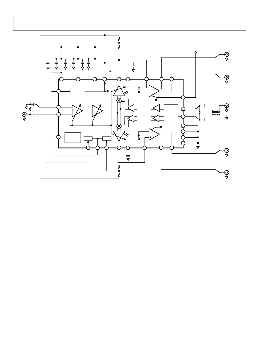
Figure 48. Adjusting AGC Level to Increase Baseband Amplifier Output Swing
CHANGING THE AGC SETPOINT
The AGC circuit can be easily set up to level at voltages higher
than the nominal 24 mV p-p, as shown in Figure 48. The
voltages on Pin IMXO and Pin QMXO are attenuated before
being applied to the detector inputs. In the example shown, an
attenuation factor of 0.2 (14 dB) between IMXO and QMXO
and the detector inputs causes the VGA to level at approximately
120 mV p-p (note that the resistor divider network must be
referenced to VVREF). This results in a peak-to-peak output
swing at the baseband amplifier outputs of 3.8 V differential,
that is, 1.6 V to 3.4 V on each side. Note that VVCMO has been
increased to 2.5 V to avoid signal clipping at the baseband
outputs. Due to the attenuation between the mixer output and
the detector input, the variation in the settled mixer output level
vs. RF input power will be greater than the variation shown in
Figure 34. The variation will be greater by a factor equal to the
inverse of the attenuation factor.
BASEBAND AMPLIFIERS
The final baseband amplifier stage takes the signals from IMXO
and QMXO and amplifies them by 30 dB, or a factor of 31.6.
This results in a maximum system gain of 69.5 dB. When the
VGA is in AGC mode, the baseband I and Q outputs (IOPN,
IOPP, QOPN, and QOPP) deliver a differential voltage of
approximately 760 mV p-p (380 mV p-p on each side).
The single-ended input signal to the baseband amplifiers is
applied at IAIN and QAIN, the high impedance inputs. As
shown in Figure 46, the baseband amplifier operates internally
as a differential amplifier, with the second input driven by VVREF.
Therefore, bias the input signal to the baseband amplifier at VVREF.
The output common-mode level of the baseband amplifiers is
set by the voltage on Pin 5, VCMO. Connect this pin to VREF
(Pin 14) or to an external reference voltage from a device such
as an analog-to-digital converter (ADC). VVCMO has a nominal
range from 0.5 V to 2.5 V. However, since the baseband amplifiers
can only swing down to 0.4 V, higher values of VVCMO are gener-
ally required to avoid low end signal clipping. Alternatively, the
positive swing at each output is limited to 1.3 V below the
supply voltage; therefore, the maximum p-p swing is given by
2 × (VPS 1.3 0.4) V differentially.
For example, for the baseband output amplifier to deliver an
output swing of 2 V p-p (1 V p-p on each side), VVCMO must be
in a range from 0.9 V to 2.5 V.
相关PDF资料 |
PDF描述 |
|---|---|
| AD8349AREZ-RL7 | 700 MHz - 2700 MHz RF/MICROWAVE QPSK MODULATOR |
| AD8349AREZ-REEL7 | 700 MHz - 2700 MHz RF/MICROWAVE QPSK MODULATOR |
| AD8350ARMZ20 | 1000 MHz RF/MICROWAVE WIDE BAND MEDIUM POWER AMPLIFIER |
| AD8350ARZ20 | 1000 MHz RF/MICROWAVE WIDE BAND MEDIUM POWER AMPLIFIER |
| AD8350ARZ15-REEL7 | 1000 MHz RF/MICROWAVE WIDE BAND MEDIUM POWER AMPLIFIER |
相关代理商/技术参数 |
参数描述 |
|---|---|
| AD8347-EVAL | 制造商:Analog Devices 功能描述:EVALUATION BOARD ((NS)) |
| ad8347-evalz | 制造商:Analog Devices 功能描述:EVAL BD 0.8 GHZ TO 2.7 GHZ DIRECT CONVERSION QUADRATURE DEMO - Bulk |
| AD8348 | 制造商:AD 制造商全称:Analog Devices 功能描述:400 MHz to 6 GHz Broadband Quadrature Modulator |
| AD8348ARE | 制造商:Analog Devices 功能描述:QUADRATURE MODULATOR - Rail/Tube |
| AD8348ARU | 功能描述:IC QUADRATUR DEMOD 50MHZ 28TSSOP RoHS:否 类别:RF/IF 和 RFID >> RF 解调器 系列:- 产品培训模块:Lead (SnPb) Finish for COTS Obsolescence Mitigation Program 标准包装:2,500 系列:- 功能:解调器 LO 频率:- RF 频率:70MHz ~ 300MHz P1dB:-9dBm 增益:- 噪音数据:6.36dB 电流 - 电源:41.5mA 电源电压:2.7 V 封装/外壳:28-WFQFN 裸露焊盘 供应商设备封装:28-TQFN-EP(5x5) 包装:带卷 (TR) |
发布紧急采购,3分钟左右您将得到回复。