- 您现在的位置:买卖IC网 > PDF目录97841 > AD8347ARUZ-REEL7 (ANALOG DEVICES INC) 800 MHz - 2700 MHz RF/MICROWAVE QUADRAPHASE DEMODULATOR PDF资料下载
参数资料
| 型号: | AD8347ARUZ-REEL7 |
| 厂商: | ANALOG DEVICES INC |
| 元件分类: | 调制器/解调器 |
| 英文描述: | 800 MHz - 2700 MHz RF/MICROWAVE QUADRAPHASE DEMODULATOR |
| 封装: | MO-153AE, RU-28, TSSOP-28 |
| 文件页数: | 25/28页 |
| 文件大小: | 623K |
| 代理商: | AD8347ARUZ-REEL7 |
第1页第2页第3页第4页第5页第6页第7页第8页第9页第10页第11页第12页第13页第14页第15页第16页第17页第18页第19页第20页第21页第22页第23页第24页当前第25页第26页第27页第28页
AD8347
Rev. A | Page 6 of 28
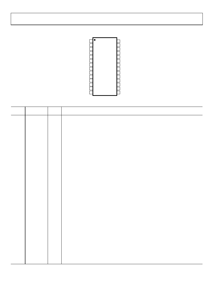
PIN CONFIGURATION AND FUNCTION DESCRIPTIONS
RFIN
VREF
RFIP
VPS2
IMXO
COM3
IOPP
IOFS
IOPN
VCMO
VPS1
LOIN
IAIN
COM2
VDT2
QMXO
QOPP
QOFS
QOPN
VAGC
COM3
VGIN
ENBL
LOIP
COM1
VDT1
QAIN
VPS3
28
27
26
25
24
23
22
21
20
19
18
17
16
15
1
2
3
4
5
6
7
8
9
10
11
12
13
14
AD8347
TOP VIEW
(Not to Scale)
02675-002
Figure 2. 28-Lead TSSOP Pin Configuration
Table 3. Pin Function Descriptions
Equiv.
Circuit
Pin No.
Mnemonic
Description
1, 28
LOIN, LOIP
A
LO Input. For optimum performance, these inputs are differentially driven. Typical input drive level is
equal to 8 dBm. To improve the match to a 50 Ω source, connect a 200 Ω shunt resistor between LOIP
and LOIN. A single-ended drive is possible, but slightly increases LO leakage.
2
VPS1
Positive Supply for LO Section. Decouple VPS1 with 0.1 μF and 100 pF capacitors.
3, 4
IOPN, IOPP
B
I-Channel Differential Baseband Output. Typical output swing is equal to 760 mV p-p differential in
AGC mode. The common-mode level on these pins is programmed by the voltage on VCMO.
5
VCMO
C
Baseband Amplifier Common-Mode Voltage. The voltage applied to this pin sets the output common-
mode level of the baseband amplifiers. This pin can either be connected to VREF (Pin 14) or to a
reference voltage from another device (typically an ADC).
6
IAIN
D
I-Channel Baseband Amplifier Input. This pin, which has a high input impedance, should be biased to
VREF (approximately 1 V). If IAIN is connected directly to IMXO, biasing is provided by IMXO. If an ac-
coupled filter is placed between IMXO and IAIN, this pin can be biased from VREF through a 1 kΩ
resistor. The gain from IAIN to the differential outputs IOPN/IOPP is 30 dB.
7, 23
COM3
Ground for Biasing and Baseband Sections.
8, 22
IMXO, QMXO
B
I-Channel and Q-Channel Baseband Mixer/VGA Outputs. Low impedance outputs with bias levels equal to
VREF. IMXO and QMXO are typically connected to IAIN and QAIN, respectively, either directly or through
filters. These outputs have a maximum current limit of about 1.5 mA. This allows for a 600 mV p-p swing into
a 200 Ω load. This corresponds to an input level of 40 dBm @ a maximum gain of 39.5 dB. At lower output
levels, IMXO and QMXO can drive a lower load resistance, subject to the same current limit.
9
COM2
RF Section Ground.
10, 11
RFIN, RFIP
E
RF Input. RFIN must be ac-coupled to ground. The RF input signal should be ac-coupled into RFIP. For
a broadband 50 Ω input impedance, connect a 200 Ω resistor from the signal side of the RFIP coupling
capacitor to ground. Note that RFIN and RFIP are not interchangeable differential inputs. RFIN is the
ground reference for the input system.
12
VPS2
Positive Supply for RF Section. Decouple VPS2 with 0.1 μF and 100 pF capacitors.
13, 16
IOFS, QOFS
F
I-Channel and Q-Channel Offset Nulling Inputs. To null the dc offset on the I-channel and Q-channel
mixer outputs (IMXO, QMXO), connect a 0.1 μF capacitor from these pins to ground. Alternately, a
forced voltage of approximately 1 V on these pins disables the offset compensation circuit.
14
VREF
G
Reference Voltage Output. This output voltage (1 V) is the main bias level for the device and can be
used to externally bias the inputs and outputs of the baseband amplifiers. The VREF pin should be
decoupled with a 0.1 μF capacitor to ground.
15
ENBL
H
Chip Enable Input. Active high.
17
VGIN
C
Gain Control Input. The voltage on this pin controls the gain on the RF and baseband VGAs. The gain
control is applied in parallel to all VGAs. The gain control voltage range is from 0.2 V to 1.2 V and
corresponds to a gain range from +39.5 dB to 30 dB. This is the gain to the output of the baseband
VGAs (that is, QMXO and IMXO). There is an additional 30 dB of gain in the baseband amplifiers. Note
that the gain control function has a negative sense (that is, increasing control voltage decreases gain).
In AGC mode, connect this pin directly to VAGC.
相关PDF资料 |
PDF描述 |
|---|---|
| AD8349AREZ-RL7 | 700 MHz - 2700 MHz RF/MICROWAVE QPSK MODULATOR |
| AD8349AREZ-REEL7 | 700 MHz - 2700 MHz RF/MICROWAVE QPSK MODULATOR |
| AD8350ARMZ20 | 1000 MHz RF/MICROWAVE WIDE BAND MEDIUM POWER AMPLIFIER |
| AD8350ARZ20 | 1000 MHz RF/MICROWAVE WIDE BAND MEDIUM POWER AMPLIFIER |
| AD8350ARZ15-REEL7 | 1000 MHz RF/MICROWAVE WIDE BAND MEDIUM POWER AMPLIFIER |
相关代理商/技术参数 |
参数描述 |
|---|---|
| AD8347-EVAL | 制造商:Analog Devices 功能描述:EVALUATION BOARD ((NS)) |
| ad8347-evalz | 制造商:Analog Devices 功能描述:EVAL BD 0.8 GHZ TO 2.7 GHZ DIRECT CONVERSION QUADRATURE DEMO - Bulk |
| AD8348 | 制造商:AD 制造商全称:Analog Devices 功能描述:400 MHz to 6 GHz Broadband Quadrature Modulator |
| AD8348ARE | 制造商:Analog Devices 功能描述:QUADRATURE MODULATOR - Rail/Tube |
| AD8348ARU | 功能描述:IC QUADRATUR DEMOD 50MHZ 28TSSOP RoHS:否 类别:RF/IF 和 RFID >> RF 解调器 系列:- 产品培训模块:Lead (SnPb) Finish for COTS Obsolescence Mitigation Program 标准包装:2,500 系列:- 功能:解调器 LO 频率:- RF 频率:70MHz ~ 300MHz P1dB:-9dBm 增益:- 噪音数据:6.36dB 电流 - 电源:41.5mA 电源电压:2.7 V 封装/外壳:28-WFQFN 裸露焊盘 供应商设备封装:28-TQFN-EP(5x5) 包装:带卷 (TR) |
发布紧急采购,3分钟左右您将得到回复。