- 您现在的位置:买卖IC网 > PDF目录10829 > AD834JRZ-RL (Analog Devices Inc)IC MULTIPLIER 4-QUADRANT 8-SOIC PDF资料下载
参数资料
| 型号: | AD834JRZ-RL |
| 厂商: | Analog Devices Inc |
| 文件页数: | 3/20页 |
| 文件大小: | 0K |
| 描述: | IC MULTIPLIER 4-QUADRANT 8-SOIC |
| 标准包装: | 2,500 |
| 功能: | 模拟乘法器 |
| 位元/级数: | 四象限 |
| 封装/外壳: | 8-SOIC(0.154",3.90mm 宽) |
| 供应商设备封装: | 8-SO |
| 包装: | 带卷 (TR) |
Data Sheet
AD834
Rev. F | Page 11 of 20
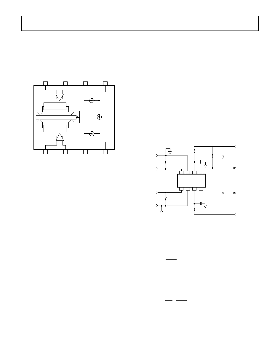
THEORY OF OPERATION
Figure 11 is a functional equivalent of the AD834. There are three
differential signal interfaces: the two voltage inputs (X = X1
X2 and Y = Y1 Y2), and the current output (W) which flows
in the direction shown in Figure 11 when X and Y are positive.
The outputs (W1 and W2) each have a standing current of
typically 8.5 mA.
00894-
010
X-DISTORTION
CANCELLATION
AD834
MULTIPLIER CORE
CURRENT
AMPLIFIER
(W)
±4mA
FS
X2
X1
+VS
W1
Y1
V-I
Y2
–VS
W2
8.5mA
8
7
5
6
1
2
3
4
Y-DISTORTION
CANCELLATION
Figure 11. Functional Block Diagram
The input voltages are first converted to differential currents
that drive the translinear core. The equivalent resistance of the
voltage-to-current (V-I) converters is about 285 Ω, which results
in low input related noise and drift. However, the low full-scale
input voltage results in relatively high nonlinearity in the V-I
converters. This is significantly reduced by the use of distortion
cancellation circuits, which operate by Kelvin sensing the voltages
generated in the core—an important feature of the AD834.
The current mode output of the core is amplified by a special
cascode stage that provides a current gain of nominally × 1.6,
trimmed during manufacturing to set up the full-scale output
current of ±4 mA. This output appears at a pair of open collec-
tors that must be supplied with a voltage slightly above the
voltage on Pin 6. As shown in Figure 12, this can be arranged
by inserting a resistor in series with the supply to Pin 6 and
taking the load resistors to the full supply. With R3 = 60 Ω, the
voltage drop across it is about 600 mV. Using two 50 load
resistors, the full-scale differential output voltage is ±400 mV.
For best performance, the voltage on the output open-collectors
(Pin 4 and Pin 5) must be higher than the voltage on Pin 6 by
about 200 mV, as shown in Figure 12.
The full bandwidth potential of the AD834 can be realized only
when very careful attention is paid to grounding and decoupling.
The device must be mounted close to a high quality ground
plane and all lead lengths must be extremely short, in keeping
with UHF circuit layout practice. In fact, the AD834 shows
useful response to well beyond 1 GHz, and the actual upper
frequency in a typical application is usually determined by the
care with which the layout is affected. Note that R4 (in series
with the VS supply) carries about 30 mA and thus introduces a
voltage drop of about 150 mV. It is made large enough to reduce
the Q of the resonant circuit formed by the supply lead and the
decoupling capacitor. Slightly larger values can be used, particu-
larly when using higher supply voltages. Alternatively, lossy RF
chokes or ferrite beads on the supply leads may be used.
For best performance, use termination resistors at the inputs, as
shown in Figure 12. Note that although the resistive component
of the input impedance is quite high (about 25 kΩ), the input
bias current of typically 45 μA can generate significant offset
voltages if not compensated. For example, with a source and
termination resistance of 50 Ω (net source of 25 Ω) the offset is
25 Ω × 45 μA = 1.125 mV. The offset can be almost fully cancelled
by including (in this example) another 25 Ω resistor in series with
the unused input. (In Figure 12, a 25 Ω resistor would be added
from X1 to GND and Y2 to GND.) To minimize crosstalk, ground
the input pins closest to the output (X1 and Y2); the effect is
merely to reverse the phase of the X input and thus alter the
polarity of the output.
00894-
0
1
8
7
6
5
1
2
3
4
X2
X1 +VS W1
Y1
Y2
–VS W2
AD834
X-INPUT
±1V FS
Y-INPUT
±1V FS
TERMINATION
RESISTOR
TERMINATION
RESISTOR
R3
62
R4
4.7
+5V
–5V
W OUTPUT
±400mV FS
R1
49.9
R1
49.9
1F
CERAMIC
1F
CERAMIC
Figure 12. Basic Connections for Wideband Operation
TRANSFER FUNCTION
The Output Current W is the linear product of input voltages (X
and Y) divided by (1 V)2 and multiplied by the scaling current of
4 mA:
( ) mA
4
V
1
2
XY
W =
With the understanding that the inputs are specified in volts,
the following simplified expression can be used:
W = (XY)4 mA
Alternatively, the full transfer function can be written as
Ω
250
1
V
1
×
= XY
W
When both inputs are driven to their clipping level of about
1.3 V, the peak output current is roughly doubled to ±8 mA,
but distortion levels become very high.
相关PDF资料 |
PDF描述 |
|---|---|
| AD834JRZ-R7 | IC MULTIPLIER 4-QUADRANT 8-SOIC |
| MAX527DCWG+T | IC DAC 12BIT QUAD CALIB 24-SOIC |
| AD835AR-REEL7 | IC MULTIPLIER 4-QUADRANT 8-SOIC |
| MX7534JP+T | IC DAC 14BIT MPU COMP 20-PLCC |
| JB5HS04FM11N | CONN RCPT WATERPROOF 4POS |
相关代理商/技术参数 |
参数描述 |
|---|---|
| AD834S | 制造商:AD 制造商全称:Analog Devices 功能描述:500 MHz Four-Quadrant Multiplier |
| AD834SQ/883B | 功能描述:增效器/分频器 WIDEBAND MULTIPLIER IC RoHS:否 制造商:Texas Instruments 产品:Multiplier 逻辑系列: 工作电源电压: 最大工作温度:+ 85 C 最小工作温度:- 40 C 安装风格:Through Hole 封装 / 箱体:PDIP-14 |
| AD835 | 制造商:AD 制造商全称:Analog Devices 功能描述:250 MHz, Voltage Output 4-Quadrant Multiplier |
| AD8350 | 制造商:AD 制造商全称:Analog Devices 功能描述:Low Distortion 1.0 GHz Differential Amplifier |
| AD8350_01 | 制造商:AD 制造商全称:Analog Devices 功能描述:Low Distortion 1.0 GHz Differential Amplifier |
发布紧急采购,3分钟左右您将得到回复。