- 您现在的位置:买卖IC网 > PDF目录10829 > AD834JRZ-RL (Analog Devices Inc)IC MULTIPLIER 4-QUADRANT 8-SOIC PDF资料下载
参数资料
| 型号: | AD834JRZ-RL |
| 厂商: | Analog Devices Inc |
| 文件页数: | 5/20页 |
| 文件大小: | 0K |
| 描述: | IC MULTIPLIER 4-QUADRANT 8-SOIC |
| 标准包装: | 2,500 |
| 功能: | 模拟乘法器 |
| 位元/级数: | 四象限 |
| 封装/外壳: | 8-SOIC(0.154",3.90mm 宽) |
| 供应商设备封装: | 8-SO |
| 包装: | 带卷 (TR) |
Data Sheet
AD834
Rev. F | Page 13 of 20
00
89
4-
01
3
87
65
12
34
X2
X1 +VS W1
Y1 Y2 –VS W2
AD834
X-INPUT
±1V FS
Y-INPUT
±1V FS
TERMINATION
RESISTOR
TERMINATION
RESISTOR
+5V
RW RW
1.5RW
RL
4.7
–5V
1F
CERAMIC
1F
CERAMIC
COUTPUT
BALUN
SEE
TEXT
C
Figure 17. Using a Balun at the Output
Note that the upper bandwidth limit of the balun is determined
only by the quality of the transmission line; therefore, the upper
bandwidth of the balun usually exceeds that of the multiplier.
This is unlike a conventional transformer where the signal is
conveyed as a flux in a magnetic core and is limited by core
losses and leakage inductance. The lower limit on bandwidth is
determined by the series inductance of the line, taken as a
whole, and the load resistance (if the blocking capacitors, C, are
sufficiently large). In practice, a balun can provide excellent
differential-to-single-sided conversion over much wider
bandwidths than a transformer.
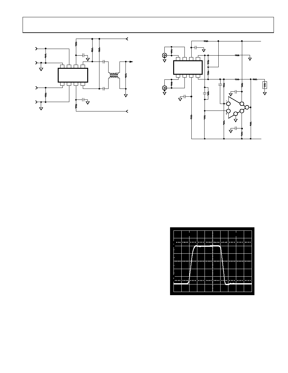
WIDEBAND MULTIPLIER CONNECTIONS
When operation down to dc and a ground based output are
necessary, the configuration shown in Figure 18 can be used.
The element values were chosen in this example to result in a
full-scale output of ±1 V at the load, so the overall multiplier
transfer function is
W = (X1 X2)(Y1 Y2)
where the X1, X2, Y1, Y2 inputs and W output are in volts. The
polarity of the output can be reversed simply by reversing either
the X or Y input.
0089
4-
014
87
6
5
12
3
4
X2
X1 +VS W1
Y1 Y2 –VS W2
AD834
49.9
0.1F
+5V
4.7
–5V
49.9
X
±1V
Y
±1V
3.01k
49.9
167
0.01F
3.01k
261
3.74k
1F
2.7
90.9
LOAD
49.9
7
3
10
1
8
14
OP AMP
Figure 18. Sideband DC-Coupled Multiplier
Choose the op amp to support the desired output bandwidth.
The op amp originally used in Figure 18 was the AD5539,
providing an overall system bandwidth of 100 MHz. The
AD8009 should provide similar performance. Many other
choices are possible where lower post multiplication band-
widths are acceptable. The level shifting network places the
input nodes of the op amp to within a few hundred millivolts of
ground using the recommended balanced supplies. The output
offset can be nulled by including a 100 Ω trim pot between each
of the lower pair of resistors (3.74 kΩ) and the negative supply.
The pulse response for this circuit is shown in Figure 19; the
X input is a pulse of 0 V to 1 V and the Y input is 1 V dc. The
transition times at the output are about 4 ns.
00
89
4-
01
5
10
0%
100
90
10ns
200mV
Figure 19. Pulse Response for the Circuit of Figure 18
相关PDF资料 |
PDF描述 |
|---|---|
| AD834JRZ-R7 | IC MULTIPLIER 4-QUADRANT 8-SOIC |
| MAX527DCWG+T | IC DAC 12BIT QUAD CALIB 24-SOIC |
| AD835AR-REEL7 | IC MULTIPLIER 4-QUADRANT 8-SOIC |
| MX7534JP+T | IC DAC 14BIT MPU COMP 20-PLCC |
| JB5HS04FM11N | CONN RCPT WATERPROOF 4POS |
相关代理商/技术参数 |
参数描述 |
|---|---|
| AD834S | 制造商:AD 制造商全称:Analog Devices 功能描述:500 MHz Four-Quadrant Multiplier |
| AD834SQ/883B | 功能描述:增效器/分频器 WIDEBAND MULTIPLIER IC RoHS:否 制造商:Texas Instruments 产品:Multiplier 逻辑系列: 工作电源电压: 最大工作温度:+ 85 C 最小工作温度:- 40 C 安装风格:Through Hole 封装 / 箱体:PDIP-14 |
| AD835 | 制造商:AD 制造商全称:Analog Devices 功能描述:250 MHz, Voltage Output 4-Quadrant Multiplier |
| AD8350 | 制造商:AD 制造商全称:Analog Devices 功能描述:Low Distortion 1.0 GHz Differential Amplifier |
| AD8350_01 | 制造商:AD 制造商全称:Analog Devices 功能描述:Low Distortion 1.0 GHz Differential Amplifier |
发布紧急采购,3分钟左右您将得到回复。