参数资料
| 型号: | AD8367ARUZ |
| 厂商: | Analog Devices Inc |
| 文件页数: | 8/24页 |
| 文件大小: | 0K |
| 描述: | IC AMP VGA 14TSSOP |
| 标准包装: | 96 |
| 系列: | X-AMP® |
| 放大器类型: | 可变增益 |
| 电路数: | 1 |
| -3db带宽: | 500MHz |
| 电流 - 输入偏压: | 27µA |
| 电流 - 电源: | 26mA |
| 电压 - 电源,单路/双路(±): | 2.7 V ~ 5.5 V |
| 工作温度: | -40°C ~ 85°C |
| 安装类型: | 表面贴装 |
| 封装/外壳: | 14-TSSOP(0.173",4.40mm 宽) |
| 供应商设备封装: | 14-TSSOP |
| 包装: | 管件 |
| 产品目录页面: | 775 (CN2011-ZH PDF) |
AD8367
Rev. A | Page 16 of 24
held to within 0.1 dB of the setpoint for >35 dB range of
input levels.
The dynamics of this loop are controlled by CAGC acting in
conjunction with an on-chip equivalent resistance, RAGC, of
10 kΩ which form an effective time-constant TAGC = RAGC CAGC.
The loop thus operates as a single-pole system with a loop
bandwidth of 1/(2π TAGC). Because the gain control function is
linear in decibels, this bandwidth is independent of the absolute
signal level. Figure 36 illustrates the loop dynamics for a 30 dB
change in input signal level with CAGC = 100 pF.
–1.2
–2.2
–2.1
–2.0
–1.9
–1.8
–1.7
–1.6
–1.5
–1.4
–1.3
–50
–40
–30
–20
–10
0
10
02710-035
PIN (dBm re 200
Ω)
P
O
UT
(dBm
re
2
0
Ω
)
Figure 35. Leveling Accuracy of the AGC Function
1.0
VAGC
VOUT
–0.6
–0.4
–0.2
0
0.2
0.4
0.6
0.8
0
5
10
15
20
25
30
35
40
02710-036
TIME (
μs)
V
ACG
(V
);
V
OUT
(a
rb)
Figure 36. AGC Response to a 32 dB Step in Input Level (f = 50 MHz)
It is important to understand that RAGC does not act as if in
shunt with CAGC. Rather, the error-correction process is that of a
true integrator, to guarantee an output that is exactly equal in
rms amplitude to the specified setpoint. For large changes in
input level, the integrating action of this loop is most apparent.
The slew rate of VAGC is determined by the peak output current
from the detector and the capacitor. Thus, for a representative
value of CAGC = 3 nF, this rate is about 20 V rms or 10 dB/μs,
while the small-signal bandwidth is 1 kHz.
Most AGC loops incorporating a true error-integrating
technique have a common weakness. When driven from an
increasingly larger signal, the AGC bias increases to reduce the
gain. However, eventually the gain falls to its minimum value,
for which further increase in this bias has no effect on the gain.
That is, the voltage on the loop capacitor is forced progressively
higher because the detector output is a current, and the AGC
bias is its integral. Consequently, there is always a precipitous
increase in this bias voltage when the input to the AD8367
exceeds that value that overdrives the detector, and because the
minimum gain is 2.5 dB, that happens for all inputs 2.5 dB
greater than the setpoint of ~350 mV rms. If possible, the user
should ensure that this limitation is preserved, preferably with a
guard-band of 5 dB to 10 dB below overload
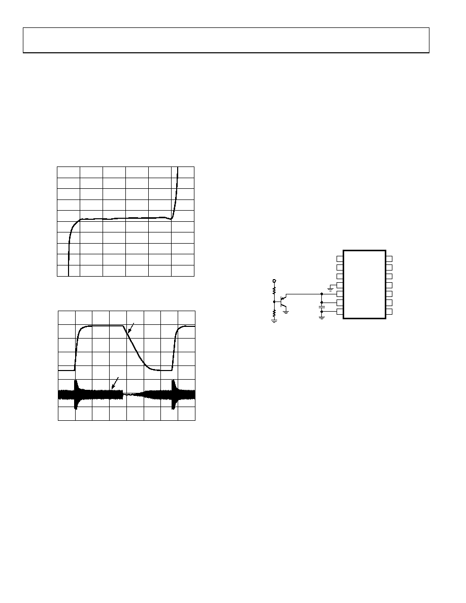
In some cases, if driven into AGC overload, the AD8367
requires unusually long times to recover; that is, the voltage
at DETO remains at an abnormally high value and the gain is at
its lowest value. To avoid this situation, it is recommended that
a clamp be placed on the DETO pin, as shown in Figure 37.
02710-037
AD8367
1
14
2
13
3
12
MODE
4
11
GAIN
5
10
DETO
6
9
ICOM
7
8
RB
RA
CAGC
0.1
μF
VAGC
Q1
2N2907
0.5V
+VS
Figure 37. External Clamp to Prevent AGC Overload.
The resistive divider network, RA and RB, should be designed
such that the base of Q1 is driven to 0.5 V.
MODIFYING THE AGC SETPOINT
If an AGC setpoint other than the internal one is desired, an
external detector must be used. Figure 38 shows a method
that uses an external true-rms detector and error integrator to
operate the AD8367 as a closed-loop AGC system with a user-
settable operating level.
The AD8361 (U2) produces a dc output level that is
proportional to the rms value of its input, taken as a sample
of the AD8367 (U1) output. This dc voltage is compared to
an externally-supplied setpoint voltage, and the difference is
integrated by the AD820 (U3) to form the gain control voltage
that is applied to the GAIN input of the AD8367 through the
divider composed of R4 and R5. This divider is included in
order to minimize overload recovery time of the loop by having
the integrator saturate at a point that only slightly overdrives the
gain control input of the AD8367. The scale factor at VAGC is
influenced by the values of R4 and R5; for the values shown, the
factor is 86 mV/dB.
相关PDF资料 |
PDF描述 |
|---|---|
| LT1994MPDD#PBF | IC OP AMP I/O DIFF LN 8-DFN |
| PBC08SBCN | CONN HEADER .100 SINGL R/A 8POS |
| PEC27SBAN | CONN HEADER .100 SINGL R/A 27POS |
| OP413FSZ-REEL | IC OPAMP GP 3.4MHZ QUAD 16SOIC |
| 929835-01-17 | CONN HEADER .100 SNGL R/A 17POS |
相关代理商/技术参数 |
参数描述 |
|---|---|
| AD8367ARUZ | 制造商:Analog Devices 功能描述:PROGRAMMABLE GAIN AMPLIFIER IC ((NW)) |
| AD8367ARUZ | 制造商:Analog Devices 功能描述:IC DETECTOR |
| AD8367ARUZ1 | 制造商:AD 制造商全称:Analog Devices 功能描述:500 MHz, Linear-in-dB VGA with AGC Detector |
| AD8367ARUZ-RL7 | 功能描述:IC AMP VGA 14TSSOP RoHS:是 类别:集成电路 (IC) >> Linear - Amplifiers - Instrumentation 系列:X-AMP® 标准包装:150 系列:- 放大器类型:音频 电路数:2 输出类型:- 转换速率:5 V/µs 增益带宽积:12MHz -3db带宽:- 电流 - 输入偏压:100nA 电压 - 输入偏移:500µV 电流 - 电源:6mA 电流 - 输出 / 通道:50mA 电压 - 电源,单路/双路(±):4 V ~ 32 V,±2 V ~ 16 V 工作温度:-40°C ~ 85°C 安装类型:表面贴装 封装/外壳:8-TSSOP(0.173",4.40mm 宽) 供应商设备封装:8-TSSOP 包装:管件 |
| AD8367-EVAL | 制造商:Analog Devices 功能描述:Evaluation Kit For 500 MHz, Linear-In-DB VGA With AGC Detector 制造商:Analog Devices 功能描述:AD8367 EVALUATION BOARD - Bulk 制造商:Analog Devices 功能描述:SEMICONDUCTOR ((NS)) |
发布紧急采购,3分钟左右您将得到回复。