参数资料
| 型号: | AD8367ARUZ |
| 厂商: | Analog Devices Inc |
| 文件页数: | 9/24页 |
| 文件大小: | 0K |
| 描述: | IC AMP VGA 14TSSOP |
| 标准包装: | 96 |
| 系列: | X-AMP® |
| 放大器类型: | 可变增益 |
| 电路数: | 1 |
| -3db带宽: | 500MHz |
| 电流 - 输入偏压: | 27µA |
| 电流 - 电源: | 26mA |
| 电压 - 电源,单路/双路(±): | 2.7 V ~ 5.5 V |
| 工作温度: | -40°C ~ 85°C |
| 安装类型: | 表面贴装 |
| 封装/外壳: | 14-TSSOP(0.173",4.40mm 宽) |
| 供应商设备封装: | 14-TSSOP |
| 包装: | 管件 |
| 产品目录页面: | 775 (CN2011-ZH PDF) |
AD8367
Rev. A | Page 17 of 24
0
2710-
038
VOUT 10
DECL 9
OCOM 8
C5
10nF
GAIN
5
DETO
6
ICOM
7
Vg
R5
10k
Ω
AD8367
U1
ICOM
1
ICOM 14
ENBL
2
HPFL 13
INPT
3
VPSI 12
MODE
4
VPSO 11
INPUT
J1
10nF
R6
57.6
Ω
CHP
10nF
RHP
100
Ω
VAGC
AD820
U3
2
3
6
4
7
VSET
5V
0.1
μF
R3
82k
Ω
20pF
C1
3.3nF
AD8361
U2
PWDN
4
COMM
5
RFIN
3
FLTR
6
IREF
2
VRMS 7
VPOS
1
SREF
8
R2
150k
Ω
R4
33k
Ω
R1
200k
Ω
10nF
0.1
μF
2.2
Ω
12k
Ω
C2
0.27
μF
Vrms
VOUT INTO A
200
Ω LOAD
5V
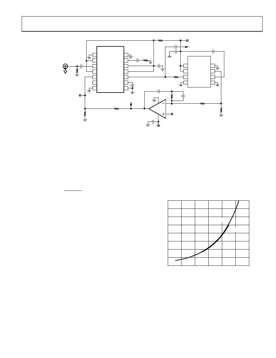
Figure 38. Example of Using an External Detector to Form an AGC Loop
Note that in this circuit the AD8367’s MODE pin must be
pulled high to obtain correct feedback polarity because the
integrator inverts the polarity of the feedback signal.
The relationship between the setpoint voltage and the rms
output voltage of the AD8367 is
(
)
7.5
225
×
+
×
=
R1
V
SET
RMS
OUT
(6)
where 225 is the input resistance of the AD8361 and 7.5 is its
conversion gain. For R1 = 200 Ω, this reduces to VOUT –RMS = VSET
× 0.25.
Capacitor C2 sets the averaging time for the rms detector. This
should be made long enough to provide sufficient smoothing of
the detector’s output in the presence of the modulation on the
RF signal. A level fluctuation of less than 1 dB (<5% to 10%) p-p
at the AD8361’s output is a reasonable value. A considerably
longer time constant needlessly lowers the AGC bandwidth,
while a short time constant can degrade the accuracy of the
true-rms measurement process. Components C1, R2, and R3
set the control loop’s bandwidth and stability. The maximum
stable loop bandwidth is limited by the rms detector’s averaging
time constant as previously discussed.
For an input signal consisting of a 4.096 MS/s QPSK modulated
carrier, the relationship between VSET and the output power for
this setup is shown in Figure 39. The exponential shape reflects
the linear-in-magnitude response of the AD8361. The adjacent
channel power ratio (ACPR) as a function of output power is
illustrated in Figure 40. The minima occur where the distortion
and integrated noise powers cross over.
The component values shown in Figure 38 were chosen for a
64-QAM signal at 500 kS/s at a carrier frequency of 150 MHz.
The response time of the loop as shown is roughly 5 ms for
an abrupt input level change of 40 dB. Figure 41 shows the
dynamic performance of the loop with a step-modulated
CW signal applied to the input for a VSET of about 1 V.
For a linear-in-dB response, detectors such as the AD8318 or
the AD8362 can be used in place of the AD8361.
4.0
3.5
3.0
2.5
2.0
1.5
1.0
0.5
0
–20
10
5
0
–5
–10
–15
02710-039
V
SET
(V
)
10MHz
380MHz
POUT (dBm INTO 200
Ω)
Figure 39. AGC Setpoint Voltage vs. Output Power
(QPSK: 4.096 MS/s; α = 0.22; 1 User)
相关PDF资料 |
PDF描述 |
|---|---|
| LT1994MPDD#PBF | IC OP AMP I/O DIFF LN 8-DFN |
| PBC08SBCN | CONN HEADER .100 SINGL R/A 8POS |
| PEC27SBAN | CONN HEADER .100 SINGL R/A 27POS |
| OP413FSZ-REEL | IC OPAMP GP 3.4MHZ QUAD 16SOIC |
| 929835-01-17 | CONN HEADER .100 SNGL R/A 17POS |
相关代理商/技术参数 |
参数描述 |
|---|---|
| AD8367ARUZ | 制造商:Analog Devices 功能描述:PROGRAMMABLE GAIN AMPLIFIER IC ((NW)) |
| AD8367ARUZ | 制造商:Analog Devices 功能描述:IC DETECTOR |
| AD8367ARUZ1 | 制造商:AD 制造商全称:Analog Devices 功能描述:500 MHz, Linear-in-dB VGA with AGC Detector |
| AD8367ARUZ-RL7 | 功能描述:IC AMP VGA 14TSSOP RoHS:是 类别:集成电路 (IC) >> Linear - Amplifiers - Instrumentation 系列:X-AMP® 标准包装:150 系列:- 放大器类型:音频 电路数:2 输出类型:- 转换速率:5 V/µs 增益带宽积:12MHz -3db带宽:- 电流 - 输入偏压:100nA 电压 - 输入偏移:500µV 电流 - 电源:6mA 电流 - 输出 / 通道:50mA 电压 - 电源,单路/双路(±):4 V ~ 32 V,±2 V ~ 16 V 工作温度:-40°C ~ 85°C 安装类型:表面贴装 封装/外壳:8-TSSOP(0.173",4.40mm 宽) 供应商设备封装:8-TSSOP 包装:管件 |
| AD8367-EVAL | 制造商:Analog Devices 功能描述:Evaluation Kit For 500 MHz, Linear-In-DB VGA With AGC Detector 制造商:Analog Devices 功能描述:AD8367 EVALUATION BOARD - Bulk 制造商:Analog Devices 功能描述:SEMICONDUCTOR ((NS)) |
发布紧急采购,3分钟左右您将得到回复。