- 您现在的位置:买卖IC网 > PDF目录5727 > AD843JRZ-16-REEL7 (Analog Devices Inc)IC OPAMP GP 34MHZ 50MA 16SOIC PDF资料下载
参数资料
| 型号: | AD843JRZ-16-REEL7 |
| 厂商: | Analog Devices Inc |
| 文件页数: | 11/12页 |
| 文件大小: | 0K |
| 描述: | IC OPAMP GP 34MHZ 50MA 16SOIC |
| 标准包装: | 250 |
| 放大器类型: | 通用 |
| 电路数: | 1 |
| 转换速率: | 250 V/µs |
| 增益带宽积: | 34MHz |
| 电流 - 输入偏压: | 50pA |
| 电压 - 输入偏移: | 1000µV |
| 电流 - 电源: | 12mA |
| 电流 - 输出 / 通道: | 50mA |
| 电压 - 电源,单路/双路(±): | ±4.5 V ~ 18 V |
| 工作温度: | 0°C ~ 70°C |
| 安装类型: | 表面贴装 |
| 封装/外壳: | 16-SOIC(0.295",7.50mm 宽) |
| 供应商设备封装: | 16-SOIC W |
| 包装: | 带卷 (TR) |
REV. D
–8–
AD843
GROUNDING AND BYPASSING
In designing practical circuits using the AD843, the user must
keep in mind that some special precautions are needed when
dealing with high frequency signals. Circuits must be wired us-
ing short interconnect leads. Ground planes should be used
whenever possible to provide both a low resistance, low induc-
tance circuit path and to minimize the effects of high frequency
coupling. IC sockets should be avoided, since their increased
interlead capacitance can degrade the bandwidth of the device.
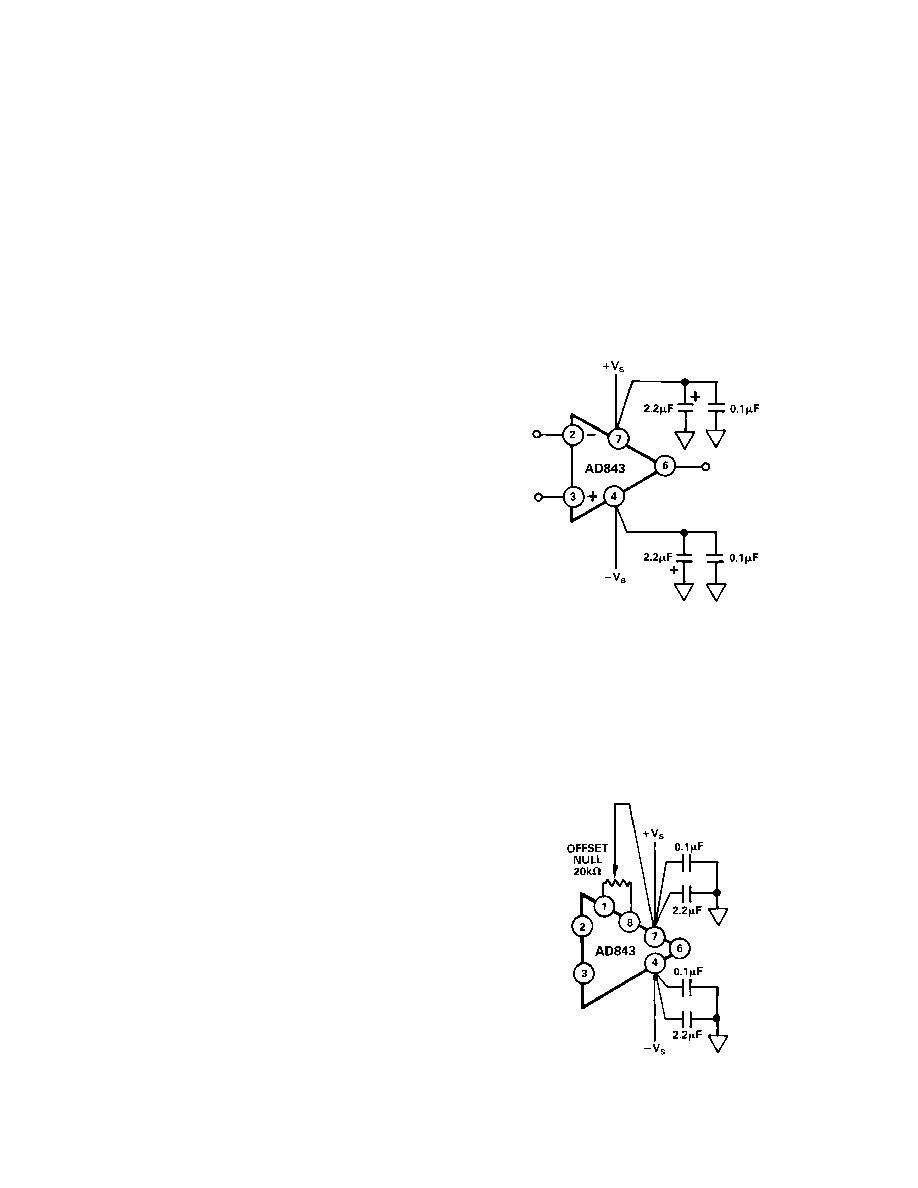
Power supply leads should be bypassed to ground as close as
possible to the pins of the amplifier. Again, the component leads
should be kept very short. As shown in Figure 24, a parallel
combination of a 2.2
F tantalum and a 0.1 F ceramic disc ca-
pacitor is recommended.
Figure 24. Recommended Power Supply Bypassing for
the AD843 (DIP Pinout)
USING A HEAT SINK
The AD843 consumes less quiescent power than most precision
high speed amplifiers and is specified to operate without using a
heat sink. However, when driving low impedance loads, the cur-
rent applied to the load can be 4 to 5 times greater than the qui-
escent current. This will produce a noticeable temperature rise,
which will increase input bias currents. The use of a small heat
sink, such as the Mouser Electronics #33HS008 is recommended.
Offset Null Configuration (DIP Pinout)
GROUNDING AND BYPASSING
Like most high bandwidth amplifiers, the AD843 is sensitive to
capacitive loading. Although it will drive capacitive loads up to
20 pF without degradation of its rated performance, both an
increased capacitive load drive capability and a “cleaner”
(nonringing) pulse response can be obtained from the AD843
by using the circuits illustrated in Figures 20 to 23. The addi-
tion of a 5 pF feedback capacitor to the unity gain inverter con-
nection (Figure 20a) substantially reduces the circuit’s
overshoot, even when it is driving a 110 pF load. This can be
seen by comparing the waveforms of Figures 20b through 20e.
To drive capacitive loads greater than 100 pF, the load should
be decoupled from the amplifier’s output by a 10
resistor and
the feedback capacitor, CF, should be connected directly be-
tween the amplifier’s output and its inverting input (Figure
21a). When using a 15 pF feedback capacitor, this circuit can
drive 400 pF with less than 20% overshoot, as illustrated in Fig-
ures 21b and 21c. Increasing capacitor CF to 47 pF also in-
creases the capacitance drive capability to 1000 pF, at the
expense of a 10:1 reduction in bandwidth compared with the
simple unity gain inverter circuit of Figure 20a.
Unity gain voltage followers (buffers) are more sensitive to
capacitive loads than are inverting amplifiers because there is no
attenuation of the feedback signal. The AD843 can drive 10 pF
to 20 pF when connected in the basic unity gain buffer circuit
of Figure 22a.
The 1 k
resistor in series with the AD843’s noninverting input
serves two functions: first, together with the amplifier’s input
capacitance, it forms a low-pass filter which slows down the
actual signal seen by the AD843. This helps reduce ringing on
the amplifier’s output voltage. The resistor’s second function is
to limit the current into the amplifier when the differential input
voltage exceeds the total supply voltage.
The AD843 will deliver a much “cleaner” pulse response when
connected in the somewhat more elaborate follower circuit of
Figure 23a. Note the reduced overshoot in Figure 23b and 23c
as compared to Figures 22b and 22c.
For maximum bandwidth, in most applications, input and feed-
back resistors used with the AD843 should have resistance val-
ues equal to or less than 1.5 k
. Even with these low resistance
values, the resultant RC time constant formed between them
and stray circuit capacitances is large enough to cause peaking
in the amplifier’s response. Adding a small capacitor, CF, as
shown in Figures 20a to 23a will reduce this peaking and flatten
the overall frequency response. CF will normally be less than
10 pF in value.
The AD843 can drive resistive loads over the range of 500
to
∞ with no change in dynamic response. While a 499 load was
used in the circuits of Figures 20-23, the performance of these
circuits will be essentially the same even if this load is removed
or changed to some other value, such as 2 k
.
To obtain the “cleanest” possible transient response when driv-
ing heavy capacitive loads, be sure to connect bypass capacitors
directly between the power supply pins of the AD843 and
ground as outlined in “grounding and bypassing.”
相关PDF资料 |
PDF描述 |
|---|---|
| LTC1100CSW | IC INSTRMNT AMP CHOP-STBL 16SOIC |
| DF3-9P-2DS | CONN HEADER 9POS 2MM RT ANG TIN |
| AD8330ACPZ-R2 | IC AMP VGA 150MHZ LN LP 16LFCSP |
| LT1168AIS8#TRPBF | IC AMP INSTR PROG PREC LP 8SOIC |
| DF3-8P-2DS | CONN HEADER 8POS 2MM RT ANG TIN |
相关代理商/技术参数 |
参数描述 |
|---|---|
| AD843K | 制造商:AD 制造商全称:Analog Devices 功能描述:34 MHz, CBFET Fast Settling Op Amp |
| AD843KN | 制造商:Analog Devices 功能描述:OP Amp Single GP ±18V 8-Pin PDIP 制造商:Analog Devices 功能描述:AMPLIFIER IC NUMBER OF CIRCUITS:1 |
| AD843KNZ | 功能描述:IC OPAMP GP 34MHZ 50MA 8DIP RoHS:是 类别:集成电路 (IC) >> Linear - Amplifiers - Instrumentation 系列:- 标准包装:2,500 系列:- 放大器类型:通用 电路数:4 输出类型:- 转换速率:0.6 V/µs 增益带宽积:1MHz -3db带宽:- 电流 - 输入偏压:45nA 电压 - 输入偏移:2000µV 电流 - 电源:1.4mA 电流 - 输出 / 通道:40mA 电压 - 电源,单路/双路(±):3 V ~ 32 V,±1.5 V ~ 16 V 工作温度:0°C ~ 70°C 安装类型:表面贴装 封装/外壳:14-TSSOP(0.173",4.40mm 宽) 供应商设备封装:14-TSSOP 包装:带卷 (TR) 其它名称:LM324ADTBR2G-NDLM324ADTBR2GOSTR |
| AD843KNZ | 制造商:Analog Devices 功能描述:IC OP-AMP FAT SETTLING |
| AD843S | 制造商:AD 制造商全称:Analog Devices 功能描述:34 MHz, CBFET Fast Settling Op Amp |
发布紧急采购,3分钟左右您将得到回复。