- 您现在的位置:买卖IC网 > PDF目录5727 > AD843JRZ-16-REEL7 (Analog Devices Inc)IC OPAMP GP 34MHZ 50MA 16SOIC PDF资料下载
参数资料
| 型号: | AD843JRZ-16-REEL7 |
| 厂商: | Analog Devices Inc |
| 文件页数: | 12/12页 |
| 文件大小: | 0K |
| 描述: | IC OPAMP GP 34MHZ 50MA 16SOIC |
| 标准包装: | 250 |
| 放大器类型: | 通用 |
| 电路数: | 1 |
| 转换速率: | 250 V/µs |
| 增益带宽积: | 34MHz |
| 电流 - 输入偏压: | 50pA |
| 电压 - 输入偏移: | 1000µV |
| 电流 - 电源: | 12mA |
| 电流 - 输出 / 通道: | 50mA |
| 电压 - 电源,单路/双路(±): | ±4.5 V ~ 18 V |
| 工作温度: | 0°C ~ 70°C |
| 安装类型: | 表面贴装 |
| 封装/外壳: | 16-SOIC(0.295",7.50mm 宽) |
| 供应商设备封装: | 16-SOIC W |
| 包装: | 带卷 (TR) |
AD843
REV. D
–9–
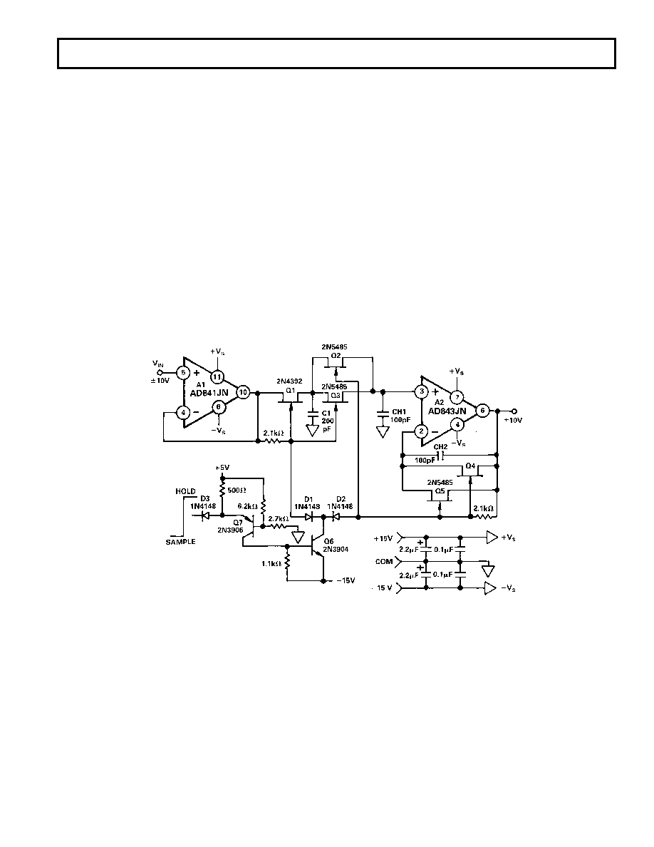
SAMPLE-AND-HOLD AMPLIFIER CIRCUITS
A Fast Switching Sample & Hold Circuit
A sample-and-hold circuit possessing short acquisition time and
low aperture delay can be built using an AD843 and discrete
JFET switches. The circuit of Figure 25 employs five n-channel
JFETs (with turn-on times of 35 ns) and an AD843 op amp
(which can settle to 0.01% in 135 ns). The circuit has an aper-
ture delay time of 50 ns and an acquisition time of 1
s or less.
This circuit is based on a noninverting open loop architecture,
using a differential hold capacitor to reduce the effects of pedes-
tal error. The charge that is removed from CH1 by Q2 and Q3
is offset by the charge removed from CH2 by Q4 and Q5. This
circuit can tolerate low hold capacitor values (approximately
100 pF), which improve acquisition time, due to the small gate-
to-drain capacitance of the discrete JFETs. Although pedestal
error will vary with input signal level, making trimming more
difficult, the circuit has the advantages of high bandwidth and
short acquisition times. In addition, it will exhibit some
nonlinearity because both amplifiers are operating with a com-
mon-mode input. Amplifier A2, however, contributes less than
0.025% linearity error, due to its 72 dB common-mode rejec-
tion ratio.
To make sure the circuit accommodates a wide
±10 V input
range, the gates of the JFETs must be connected to a potential
near the –15 V supply. The level-shift circuitry (diode D3, PNP
transistor Q7, and NPN transistor Q6) shifts the TTL level S/H
command to provide for an adequate pinch-off voltage for the
JFET switches over the full input voltage range.
The JFETs Q2, Q3, Q4 and Q5 across the two hold capacitors
ensure signal acquisition for all conditions of VIN and VOUT
when the circuit switches from the sample to the hold mode.
Transistor Q1 provides an extra stage of isolation between the
output of amplifier A1 and the hold capacitor CH1.
When selecting capacitors for use in a sample-and-hold circuit,
the designer should choose those types with low dielectric
absorption and low temperature coefficients. Silvered-mica
capacitors exhibit low (0 to 100 ppm/
°C) temperature coeffi-
cients and will still work in temperatures exceeding 200
°C. It is
also recommend that the user test the chosen capacitor to insure
that its value closely matches that printed on it since not all
capacitors are fully tested by their manufacturers for absolute
tolerance.
A high speed CB amplifier, A1, follows the input signal. U1, a
dual wideband “T” switch, connects the input buffer amp to
one of the two output amplifiers while selecting the complemen-
tary amplifier to drive the A/D input. For example, when
“select” is at logic high, A1 drives CH1, A2 tracks the input sig-
nal and the output of A3 is connected to the input of the A/D
converter. At the same time, A3 holds an analog value and its
output is connected to the input of the A/D converter. When the
select command goes to logic LOW, the two output amplifiers
alternate functions.
Since the input to the A/D converter is the alternated “held”
outputs from A1 and A2, the offset voltage mismatch of the two
amplifiers will show up as nonlinearity and, therefore, distortion
in the output signal. To minimize this, potentiometers can be
used to adjust the offsets of the output amplifiers until they are
A PING-PONG S/H AMPLIFIER
For improved throughput over the circuit of Figure 25, a “ping-
pong” architecture may be used. A ping-pong circuit overcomes
some of the problems associated with high speed S/H amplifiers
by allowing the use of a larger hold capacitor for a given sample
rate: this will reduce the associated feedthrough, droop and ped-
estal errors.
Figure 26 illustrates a simple, four-chip ping-pong sample-and-
hold amplifier circuit. This design increases throughput by using
one channel to acquire a new sample while another channel
holds the previous sample. Instead of having to reacquire the
signal when switching from hold to sample mode, it alternately
connects the outputs from Channel 1 or from Channel 2 to the
A/D converter. In this case, the throughput is the slew rate and
settling time of the output amplifiers, A2 and A3.
Figure 25. A Fast Switching Sample-and-Hold Amplifier
相关PDF资料 |
PDF描述 |
|---|---|
| LTC1100CSW | IC INSTRMNT AMP CHOP-STBL 16SOIC |
| DF3-9P-2DS | CONN HEADER 9POS 2MM RT ANG TIN |
| AD8330ACPZ-R2 | IC AMP VGA 150MHZ LN LP 16LFCSP |
| LT1168AIS8#TRPBF | IC AMP INSTR PROG PREC LP 8SOIC |
| DF3-8P-2DS | CONN HEADER 8POS 2MM RT ANG TIN |
相关代理商/技术参数 |
参数描述 |
|---|---|
| AD843K | 制造商:AD 制造商全称:Analog Devices 功能描述:34 MHz, CBFET Fast Settling Op Amp |
| AD843KN | 制造商:Analog Devices 功能描述:OP Amp Single GP ±18V 8-Pin PDIP 制造商:Analog Devices 功能描述:AMPLIFIER IC NUMBER OF CIRCUITS:1 |
| AD843KNZ | 功能描述:IC OPAMP GP 34MHZ 50MA 8DIP RoHS:是 类别:集成电路 (IC) >> Linear - Amplifiers - Instrumentation 系列:- 标准包装:2,500 系列:- 放大器类型:通用 电路数:4 输出类型:- 转换速率:0.6 V/µs 增益带宽积:1MHz -3db带宽:- 电流 - 输入偏压:45nA 电压 - 输入偏移:2000µV 电流 - 电源:1.4mA 电流 - 输出 / 通道:40mA 电压 - 电源,单路/双路(±):3 V ~ 32 V,±1.5 V ~ 16 V 工作温度:0°C ~ 70°C 安装类型:表面贴装 封装/外壳:14-TSSOP(0.173",4.40mm 宽) 供应商设备封装:14-TSSOP 包装:带卷 (TR) 其它名称:LM324ADTBR2G-NDLM324ADTBR2GOSTR |
| AD843KNZ | 制造商:Analog Devices 功能描述:IC OP-AMP FAT SETTLING |
| AD843S | 制造商:AD 制造商全称:Analog Devices 功能描述:34 MHz, CBFET Fast Settling Op Amp |
发布紧急采购,3分钟左右您将得到回复。