- 您现在的位置:买卖IC网 > PDF目录10791 > AD8522AR-REEL (Analog Devices Inc)IC DAC DUAL 12BIT 5V 14-SOIC PDF资料下载
参数资料
| 型号: | AD8522AR-REEL |
| 厂商: | Analog Devices Inc |
| 文件页数: | 5/8页 |
| 文件大小: | 0K |
| 描述: | IC DAC DUAL 12BIT 5V 14-SOIC |
| 产品培训模块: | Data Converter Fundamentals DAC Architectures |
| 产品变化通告: | AD8522 Redesign Change 29/Nov/2010 Product Discontinuance 27/Oct/2011 |
| 标准包装: | 2,500 |
| 设置时间: | 16µs |
| 位数: | 12 |
| 数据接口: | 串行 |
| 转换器数目: | 2 |
| 电压电源: | 单电源 |
| 功率耗散(最大): | 25mW |
| 工作温度: | -40°C ~ 85°C |
| 安装类型: | 表面贴装 |
| 封装/外壳: | 14-SOIC(0.154",3.90mm 宽) |
| 供应商设备封装: | 14-SO |
| 包装: | 带卷 (TR) |
| 输出数目和类型: | 2 电压,单极 |
| 采样率(每秒): | 62.5k |
AD8522
REV. A
–5–
OPERATION
The AD8522 is a complete ready-to-use dual 12-bit digital-to-
analog converter. Only one +5 V power supply is necessary for
operation. It contains two voltage-switched, 12-bit, laser-
trimmed digital-to-analog converters, a curvature-corrected
bandgap reference, rail-to-rail output op amps, input registers,
and DAC registers. The serial data interface consists of a serial
data input (SDI), clock (CLK), and two load strobe pins (LDA,
LDB
) with an active low CS strobe. In addition, an asynchro-
nous RS pin will set all DAC register bits to zero causing the
VOUT to become zero volts, or to midscale for trimming applica-
tions when the MSB pin is programmed to Logic 1. This func-
tion is useful for power on reset or system failure recovery to a
known state.
D/A CONVERTER SECTION
The internal DAC is a 12-bit voltage-mode device with an out-
put that swings from AGND potential to the 2.5 V internal
bandgap voltage. It uses a laser-trimmed R-2R ladder which is
switched by N channel MOSFETs. The output voltage of the
DAC has a constant resistance independent of digital input
code. The DAC output is internally connected to the rail-to-rail
output op amp.
AMPLIFIER SECTION
The internal DAC’s output is buffered by a low power con-
sumption precision amplifier. This low power amplifier contains
a differential PNP pair input stage that provides low offset volt-
age and low noise, as well as the ability to amplify the zero-scale
DAC output voltages. The rail-to-rail amplifier is configured in
a gain of 1.638 (= 4.095 V/2.5 V) in order to set the 4.095 V
full-scale output (1 mV/LSB). See Figure 4 for an equivalent
circuit schematic of the analog section.
BUFFER
2R
R
SPDT
N CH FET
SWITCHES
2R
R2
R1
RAIL-TO-RAIL
OUTPUT
AMPLIFIER
VOUT
BANDGAP
REFERENCE
VREF
2.5V
VOLTAGE SWITCHED 12-BIT
R-2R D/A CONVERTER
AV = 4.096/2.5
= 1.638V/V
Figure 4. Equivalent AD8522 Schematic of Analog Portion
The op amp has a 16
s typical settling time to 0.01%. There
are slight differences in settling time for negative slewing signals
versus positive. See the oscilloscope photos in the “Typical Per-
formance Characteristics” section of this data sheet.
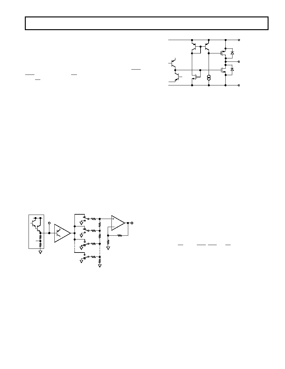
OUTPUT SECTION
The rail-to-rail output stage of this amplifier has been designed
to provide precision performance while operating near either
power supply. Figure 5 shows an equivalent output schematic of
the rail-to-rail amplifier with its N channel pull-down FETs that
will pull an output load directly to GND. The output sourcing
current is provided by a P channel pull-up device that can sup-
ply GND terminated loads, especially important at the –10%
supply tolerance value of 4.5 V.
P-CH
N-CH
VDD
VOUT
AGND
Figure 5. Equivalent Analog Output Circuit
Figures 6 and 7 in the typical performance characteristics sec-
tion provide information on output swing performance near
ground and full scale as a function of load. In addition to resis-
tive load driving capability the amplifier has also been carefully
designed and characterized for up to 500 pF capacitive load
driving capability.
REFERENCE SECTION
The internal 2.5 V curvature-corrected bandgap voltage refer-
ence is laser trimmed for both initial accuracy and low tempera-
ture coefficient. The voltage generated by the reference is
available at the VREF pin. Since VREF is not intended to drive
heavy external loads, it must be buffered. The equivalent emit-
ter follower output circuit of the VREF pin is shown in Figure 4.
Bypassing the VREF pin will improve noise performance; how-
ever, bypassing is not required for proper operation. Figure 10
shows broad band noise performance.
POWER SUPPLY
The very low power consumption of the AD8522 is a direct
result of a circuit design optimizing use of a CBCMOS process.
By using the low power characteristics of the CMOS for the
logic, and the low noise, tight matching of the complementary
bipolar transistors good analog accuracy is achieved.
For power consumption sensitive applications it is important to
note that the internal power consumption of the AD8522 is
strongly dependent on the actual input voltage levels present on
the SDI, CLK, CS, MSB, LDA, LDB and RS pins. Since these in-
puts are standard CMOS logic structures, they contribute static
power dissipation dependent on the actual driving logic VOH and
VOL voltage levels. Consequently for optimum dissipation use of
CMOS logic versus TTL provides minimal dissipation in the static
state. A VINL = 0 V on the logic input pins provides the lowest
standby dissipation of 1 mA with a +5 V power supply.
As with any analog system, it is recommended that the AD8522
power supply be bypassed on the same PC card that contains
the chip. Figure 12 shows the power supply rejection versus fre-
quency performance. This should be taken into account when
using higher frequency switched-mode power supplies with
ripple frequencies of 100 kHz and higher.
One advantage of the rail-to-rail output amplifiers used in the
AD8522 is the wide range of usable supply voltage. The part is
fully specified and tested over temperature for operation from
+4.5 V to +5.5 V. If reduced linearity and source current capa-
bility near full scale can be tolerated, operation of the AD8522
相关PDF资料 |
PDF描述 |
|---|---|
| LTC1445IDHD#PBF | IC COMP QD LP 1.221VREF 16-DFN |
| LTC488CSW#PBF | IC LINE RCVR RS485 QUAD 16-SOIC |
| VI-J41-MY-S | CONVERTER MOD DC/DC 12V 50W |
| AD8611ARZ | IC COMP SNGL 4NS ULTRFAST 8-SOIC |
| LT1394CS8#PBF | IC COMPARATOR LOW PWR 7NS 8-SOIC |
相关代理商/技术参数 |
参数描述 |
|---|---|
| AD8522ARZ | 功能描述:IC DAC 12BIT DUAL 5V 14-SOIC RoHS:是 类别:集成电路 (IC) >> 数据采集 - 数模转换器 系列:- 产品培训模块:Lead (SnPb) Finish for COTS Obsolescence Mitigation Program 标准包装:50 系列:- 设置时间:4µs 位数:12 数据接口:串行 转换器数目:2 电压电源:单电源 功率耗散(最大):- 工作温度:-40°C ~ 85°C 安装类型:表面贴装 封装/外壳:8-TSSOP,8-MSOP(0.118",3.00mm 宽) 供应商设备封装:8-uMAX 包装:管件 输出数目和类型:2 电压,单极 采样率(每秒):* 产品目录页面:1398 (CN2011-ZH PDF) |
| AD8522ARZ | 制造商:Analog Devices 功能描述:IC, DAC, 12BIT, 62.5KSPS, SOIC-14 |
| AD8522ARZ-REEL | 功能描述:IC DAC DUAL 12BIT 5V 14SOIC RoHS:是 类别:集成电路 (IC) >> 数据采集 - 数模转换器 系列:- 标准包装:47 系列:- 设置时间:2µs 位数:14 数据接口:并联 转换器数目:1 电压电源:单电源 功率耗散(最大):55µW 工作温度:-40°C ~ 85°C 安装类型:表面贴装 封装/外壳:28-SSOP(0.209",5.30mm 宽) 供应商设备封装:28-SSOP 包装:管件 输出数目和类型:1 电流,单极;1 电流,双极 采样率(每秒):* |
| AD8522JRU | 制造商:Rochester Electronics LLC 功能描述:+5V DUAL 12-BIT DAC - Bulk 制造商:Analog Devices 功能描述: |
| AD8522JRU-REEL | 制造商:Analog Devices 功能描述:DAC 2-CH R-2R 12-bit 14-Pin TSSOP T/R 制造商:Rochester Electronics LLC 功能描述:- Tape and Reel |
发布紧急采购,3分钟左右您将得到回复。