参数资料
| 型号: | AD9115BCPZ |
| 厂商: | Analog Devices Inc |
| 文件页数: | 43/52页 |
| 文件大小: | 0K |
| 描述: | IC DAC DUAL 10BIT LO PWR 40LFCSP |
| 产品培训模块: | Data Converter Fundamentals DAC Architectures |
| 标准包装: | 1 |
| 系列: | TxDAC® |
| 位数: | 10 |
| 数据接口: | 串行 |
| 转换器数目: | 2 |
| 电压电源: | 模拟和数字 |
| 功率耗散(最大): | 232mW |
| 工作温度: | -40°C ~ 85°C |
| 安装类型: | 表面贴装 |
| 封装/外壳: | 40-VFQFN 裸露焊盘,CSP |
| 供应商设备封装: | 40-LFCSP-VQ(6x6) |
| 包装: | 托盘 |
| 输出数目和类型: | 4 电流,单极 |
| 采样率(每秒): | 125M |
| 产品目录页面: | 785 (CN2011-ZH PDF) |
第1页第2页第3页第4页第5页第6页第7页第8页第9页第10页第11页第12页第13页第14页第15页第16页第17页第18页第19页第20页第21页第22页第23页第24页第25页第26页第27页第28页第29页第30页第31页第32页第33页第34页第35页第36页第37页第38页第39页第40页第41页第42页当前第43页第44页第45页第46页第47页第48页第49页第50页第51页第52页
AD9114/AD9115/AD9116/AD9117
Data Sheet
Rev. C | Page 48 of 52
DIFFERENTIAL BUFFERED OUTPUT
USING AN OP AMP
A dual op amp (see the circuit shown in Figure 104) can be
used in a differential version of the single-ended buffer shown
in Figure 103. Figure 104 is a simplified schematic. The REFIO
pin must be buffered to keep the load current less than 100 nA.
The same RC network is used to form a one-pole differential,
low-pass filter to isolate the op amp inputs from the high
frequency images produced by the DAC outputs. The feedback
resistors, RFB, determine the differential peak-to-peak signal swing
by the formula
VOUT = 2 × RFB × IFS
The maximum and minimum single-ended voltages out of the
amplifier are, respectively,
+
×
=
B
FB
REF
MAX
R
V
1
VMIN = VMAX RFB × IFS
The common-mode voltage of the differential output is
determined by the formula
VCM = VMAX RFB × IFS
AD9114/AD9115/
AD9116/AD9117
IOUTP
IOUTN
RFB
VOUT
REFIO 34
28
RS
AVSS 25
CF
C
RFB
RB
CF
RS
RB
29
+
–
ADA4841-2
+
–
ADA4841-2
07466-
065
Figure 104. Single-Supply Differential Buffer
AUXILIARY DACs
The DACs of the AD9114/AD9115/AD9116/AD9117 feature
two versatile and independent 10-bit auxiliary DACs suitable
for dc offset correction and similar tasks.
Because the AUXDACs are driven through the SPI port, they
should never be used in timing-critical applications, such as
inside analog feedback loops.
To keep the pin count reasonable, these auxiliary DACs each
share a pin with the corresponding FSADJx resistor. They are,
therefore, usable only when enabled and when that DAC is
operated on its internal full-scale resistors. A simple I-to-V
converter is implemented on-chip with selectable shunt resistors
(3.2 kΩ to 16 kΩ) such that if REFIO is set to exactly 1 V, REFIO/2
equals 0.5 V and the following equation describes the no load
output voltage:
kΩ
16
5
.
1
V
5
.
0
=
S
DAC
OUT
R
I
V
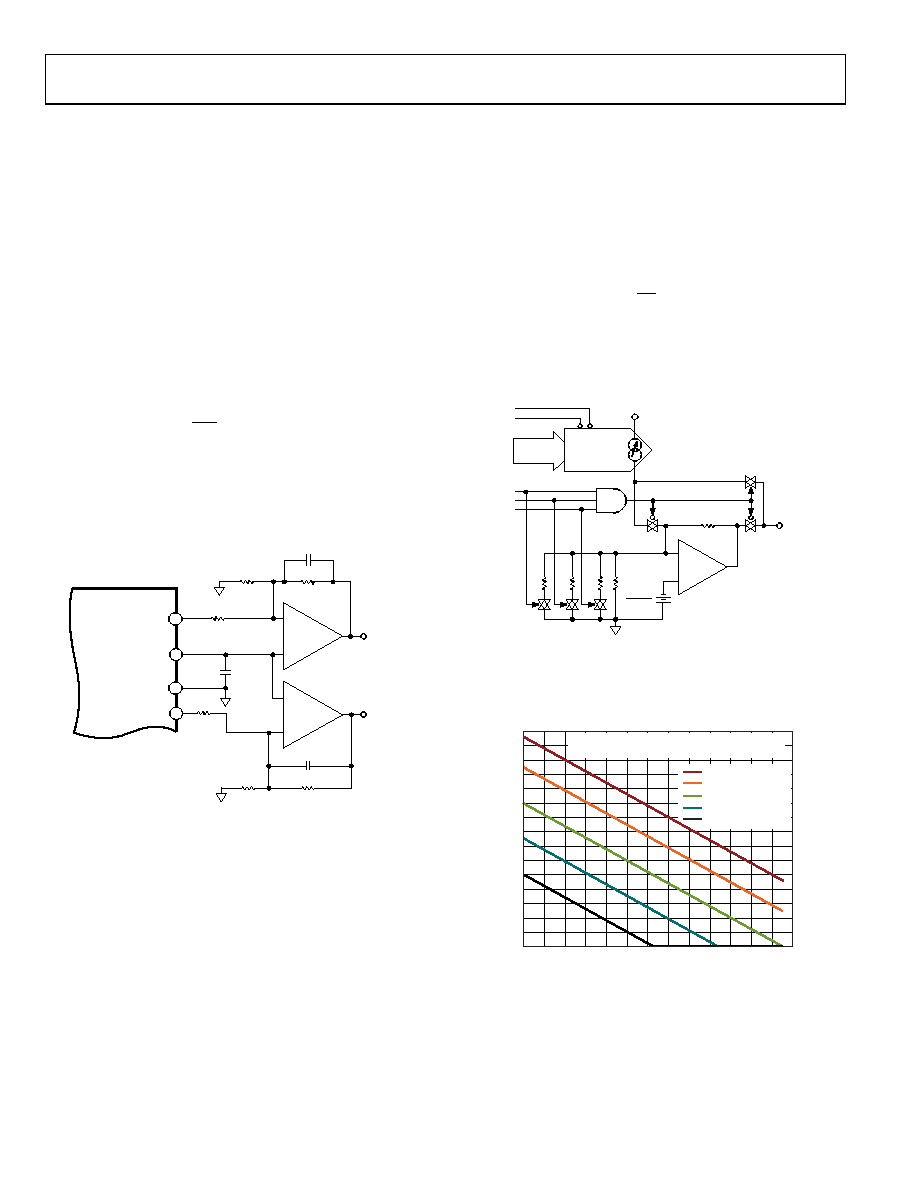
Figure 105 illustrates the function of all the SPI bits controlling
these DACs with the exception of the QAUXEN (Register 0x0A)
and IAUXEN (Register 0x0C) bits and gating to prohibit
RS < 3.2 kΩ.
+
–
OP AMP
AUXDAC
[9:0]
AVDD
RNG0
RNG1
REFIO
2
16k 16k
16k
4k 8k
OFS2
OFS1
OFS0
(OFS > 4 = 4)
AUX
PIN
RNG: 00 = 125A
fS
01 = 62A
fS
10 = 31A
fS
11 = 16A
fS
07466-
066
Figure 105. AUXDAC Simplified Circuit Diagram
The SPI speed limits the update rate of the auxiliary DACs. The
data is inverted such that IAUXDAC is full scale at 0x000 and zero
at 0x1FF, as shown in Figure 106.
3.0
2.8
2.6
2.4
2.2
2.0
1.8
1.6
1.4
1.2
1.0
0.8
0.6
0.4
0.2
0
10
20
30
40
50
60
70
80
90
100
120 130
DAC CURRENT (A)
O
U
T
PU
T
(V)
110
ROFFSET = 3.3k
ROFFSET = 4k
ROFFSET = 5.3k
ROFFSET = 8k
ROFFSET = 16k
OP AMP OUTPUT VOLTAGE vs.
CHANGES IN ROFFSET AND DAC CURRENT IN A
07466-
067
Figure 106. AUXDAC Op Amp Output vs. Current, AVDD = 3.3 V No Load,
AUXDAC 0x1FF to 0x000
相关PDF资料 |
PDF描述 |
|---|---|
| VI-B73-MY-F2 | CONVERTER MOD DC/DC 24V 50W |
| VI-JNY-MZ-F4 | CONVERTER MOD DC/DC 3.3V 16.5W |
| AD1852JRSZ | IC DAC STEREO 24BIT 5V 28-SSOP |
| VI-B72-MY-F2 | CONVERTER MOD DC/DC 15V 50W |
| SN74AVCH4T245PWT | IC BUS TRANSCVR 4BIT 16TSSOP |
相关代理商/技术参数 |
参数描述 |
|---|---|
| AD9115BCPZRL7 | 功能描述:IC DAC DUAL 10BIT LO PWR 40LFCSP RoHS:是 类别:集成电路 (IC) >> 数据采集 - 数模转换器 系列:TxDAC® 标准包装:47 系列:- 设置时间:2µs 位数:14 数据接口:并联 转换器数目:1 电压电源:单电源 功率耗散(最大):55µW 工作温度:-40°C ~ 85°C 安装类型:表面贴装 封装/外壳:28-SSOP(0.209",5.30mm 宽) 供应商设备封装:28-SSOP 包装:管件 输出数目和类型:1 电流,单极;1 电流,双极 采样率(每秒):* |
| AD9115-DPG2-EBZ | 功能描述:IC DAC DUAL 10BIT LO PWR 40LFCSP RoHS:是 类别:编程器,开发系统 >> 评估板 - 数模转换器 (DAC) 系列:TxDAC® 产品培训模块:Lead (SnPb) Finish for COTS Obsolescence Mitigation Program 标准包装:1 系列:- DAC 的数量:4 位数:12 采样率(每秒):- 数据接口:串行,SPI? 设置时间:3µs DAC 型:电流/电压 工作温度:-40°C ~ 85°C 已供物品:板 已用 IC / 零件:MAX5581 |
| AD9115-EBZ | 制造商:Analog Devices 功能描述:DUAL 10 BIT LOW POWER CONVERTER - Boxed Product (Development Kits) |
| AD9116 | 制造商:AD 制造商全称:Analog Devices 功能描述:Dual, 8-/10-/12-/14-Bit Low Power Digital-to-Analog Converters |
| AD9116BCPZ | 功能描述:IC DAC DUAL 12BIT LO PWR 40LFCSP RoHS:是 类别:集成电路 (IC) >> 数据采集 - 数模转换器 系列:TxDAC® 产品培训模块:Lead (SnPb) Finish for COTS Obsolescence Mitigation Program 标准包装:50 系列:- 设置时间:4µs 位数:12 数据接口:串行 转换器数目:2 电压电源:单电源 功率耗散(最大):- 工作温度:-40°C ~ 85°C 安装类型:表面贴装 封装/外壳:8-TSSOP,8-MSOP(0.118",3.00mm 宽) 供应商设备封装:8-uMAX 包装:管件 输出数目和类型:2 电压,单极 采样率(每秒):* 产品目录页面:1398 (CN2011-ZH PDF) |
发布紧急采购,3分钟左右您将得到回复。