- 您现在的位置:买卖IC网 > PDF目录10681 > AD9203ARUZ (Analog Devices Inc)IC ADC 10BIT 40MSPS 3V 28-TSSOP PDF资料下载
参数资料
| 型号: | AD9203ARUZ |
| 厂商: | Analog Devices Inc |
| 文件页数: | 6/28页 |
| 文件大小: | 0K |
| 描述: | IC ADC 10BIT 40MSPS 3V 28-TSSOP |
| 标准包装: | 50 |
| 位数: | 10 |
| 采样率(每秒): | 40M |
| 数据接口: | 并联 |
| 转换器数目: | 5 |
| 功率耗散(最大): | 108mW |
| 电压电源: | 模拟和数字 |
| 工作温度: | -40°C ~ 85°C |
| 安装类型: | 表面贴装 |
| 封装/外壳: | 28-TSSOP(0.173",4.40mm 宽) |
| 供应商设备封装: | 28-TSSOP |
| 包装: | 管件 |
| 输入数目和类型: | 2 个单端,单极;1 个差分,单极 |
| 产品目录页面: | 780 (CN2011-ZH PDF) |
第1页第2页第3页第4页第5页当前第6页第7页第8页第9页第10页第11页第12页第13页第14页第15页第16页第17页第18页第19页第20页第21页第22页第23页第24页第25页第26页第27页第28页
AD9203
Rev. B | Page 14 of 28
00573-025
S2
S3
S1
AD9203
CH
CP
Figure 25. Input Architecture
The structure of the input SHA places certain requirements on
the input drive source. The combination of the pin capacitance,
CP, and the hold capacitance, CH, is typically less than 5 pF. The
input source must be able to charge or discharge this
capacitance to 10-bit accuracy in one half of a clock cycle.
When the SHA goes into track mode, the input source must
charge or discharge capacitor CH from the voltage already stored
on CH to the new voltage. In the worst case, a full-scale voltage
step on the input source must provide the charging current
through the RON (100 ) of Switch 1 and quickly (within 1/2
CLK period) settle. This situation corresponds to driving a low
input impedance. Adding series resistance between the output
of the signal source and the AIN pin reduces the drive
requirements placed on the signal source. Figure 26 shows this
configuration. The bandwidth of the particular application
limits the size of this resistor. To maintain the performance
outlined in the data sheet specifications, the resistor should be
limited to 50 or less. The series input resistor can be used to
isolate the driver from the AD9203’s switched capacitor input.
The external capacitor may be selected to limit the bandwidth
into the AD9203. Two input RC networks should be used to
balance differential input drive schemes (Figure 26).
The input span of the AD9203 is a function of the reference
voltage. For more information regarding the input range, see
Operation sections of the data sheet.
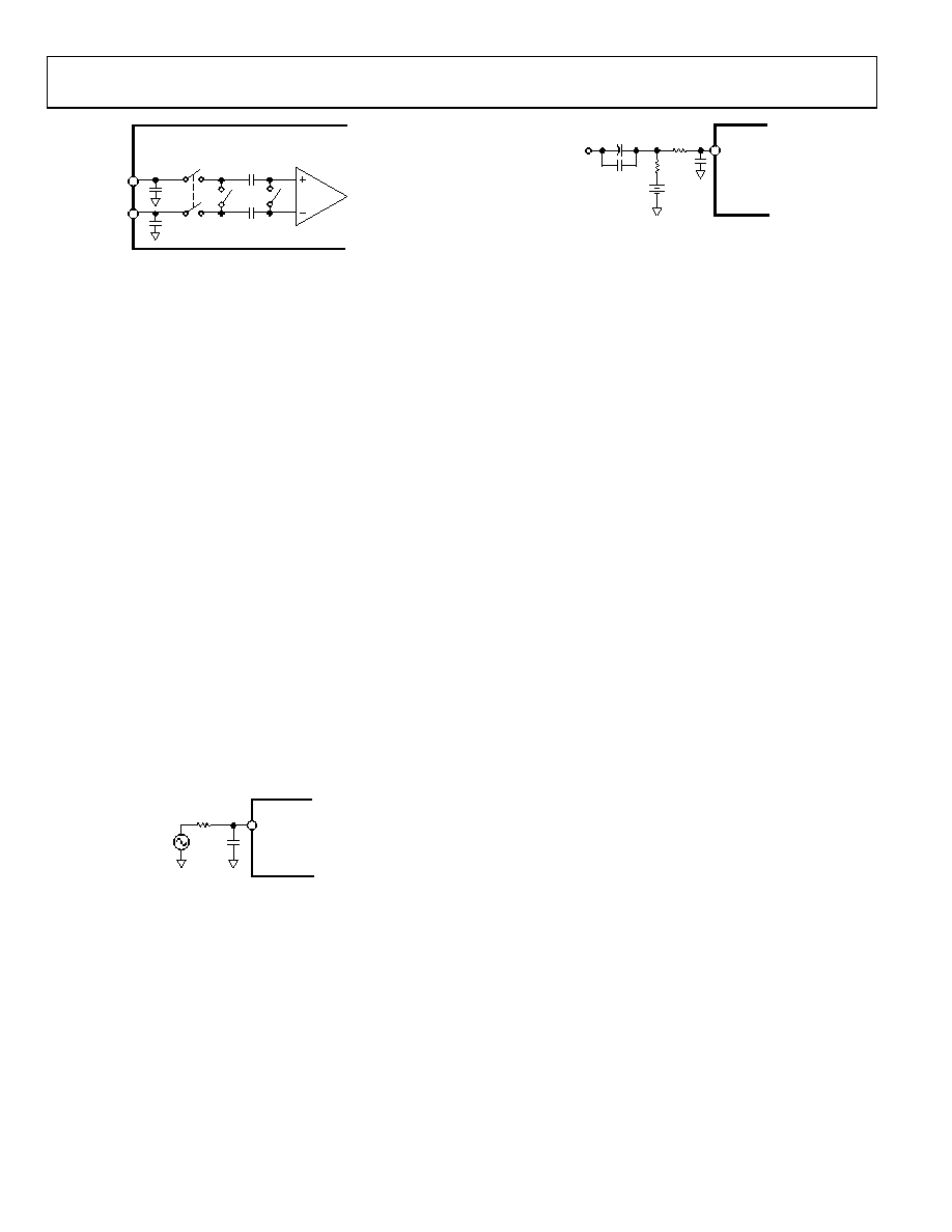
00573-026
AIN
VS
<50
AD9203
Figure 26. Simple AD9203 Drive Configuration
In many cases, particularly in single-supply operation, ac
coupling offers a convenient way of biasing the analog input
signal to the proper signal range. Figure 27 shows a typical
configuration for ac-coupling the analog input signal to the
AD9203. Maintaining the specifications outlined in the data
sheet requires careful selection of the component values. The
most important is the f–3 dB high-pass corner frequency. It is a
function of R2 and the parallel combination of C1 and C2.
00573-027
AIN
R1
R2
VBIAS
VIN
AVDD/2
+
–
C1
C2
AD9203
Figure 27. AC-Coupled Input
The f–3 dB point can be approximated by the equation:
f3dB = 1/(2π × [R2] CEQ)
where CEQ is the parallel combination of C1 and C2. Note that
C1 is typically a large electrolytic or tantalum capacitor that
becomes inductive at high frequencies. Add a small ceramic or
polystyrene capacitor (on the order of 0.01 F) that is negligibly
inductive at higher frequencies while maintaining a low
impedance over a wide frequency range.
There are additional considerations when choosing the resistor
values for an ac-coupled input. The ac-coupling capacitors
integrate the switching transients present at the input of the
AD9203 and cause a net dc bias current, IB, to flow into the
input. The magnitude of the bias current increases as the signal
changes and as the clock frequency increases. This bias current
will result in an offset error of (R1 + R2) IB. If it is necessary to
compensate for this error, consider modifying VBIAS to
account for the resultant offset. In systems that must use dc
coupling, use an op amp to level shift ground-referenced signals
to comply with the input requirements of the AD9203.
OP AMP SELECTION GUIDE
Op amp selection for the AD9203 is highly application
dependent. In general, the performance requirements of any
given application can be characterized by either time domain or
frequency domain constraints. In either case, one should
carefully select an op amp that preserves the performance of the
A/D. This task becomes challenging when one considers the
AD9203’s high performance capabilities coupled with other
system level requirements such as power consumption and cost.
The ability to select the optimal op amp may be further
complicated by either limited power supply availability and/or
limited acceptable supplies for a desired op amp. Newer, high
performance op amps typically have input and output range
limitations in accordance with their lower supply voltages. As a
result, some op amps will be more appropriate in systems where
ac coupling is allowed. When dc coupling is required, the
headroom constraints of op amps (such as rail-to-rail op amps)
or ones where larger supplies can be used, should be
considered.
The following section describes some op amps currently
available from Analog Devices. Please contact the factory or
local sales office for updates on Analog Devices latest amplifier
product offerings.
相关PDF资料 |
PDF描述 |
|---|---|
| LT1720IDD#TRPBF | IC COMPARATOR DUAL HS 3/5V 8-DFN |
| LT1720IDD#TR | IC COMPARATOR DUAL HS 3/5V 8-DFN |
| AD7277BUJZ-500RL7 | IC ADC 10BIT 3MSPS TSOT23-6 |
| LT1720IDD#PBF | IC COMPARATOR DUAL HS 3/5V 8-DFN |
| LT1720IDD | IC COMPARATOR DUAL HS 3/5V 8-DFN |
相关代理商/技术参数 |
参数描述 |
|---|---|
| AD9203ARUZ | 制造商:Analog Devices 功能描述:IC ADC 10BIT 40MSPS 28TSSOP |
| AD9203ARUZ | 制造商:Analog Devices 功能描述:IC, ADC, 10BIT, 40MSPS, TSSOP-28 |
| AD9203ARUZ1 | 制造商:AD 制造商全称:Analog Devices 功能描述:10-Bit, 40 MSPS, 3 V, 74 mW A/D Converter |
| AD9203ARUZRL7 | 功能描述:IC ADC 10BIT CMOS 40MSPS 28TSSOP RoHS:是 类别:集成电路 (IC) >> 数据采集 - 模数转换器 系列:- 标准包装:1,000 系列:- 位数:16 采样率(每秒):45k 数据接口:串行 转换器数目:2 功率耗散(最大):315mW 电压电源:模拟和数字 工作温度:0°C ~ 70°C 安装类型:表面贴装 封装/外壳:28-SOIC(0.295",7.50mm 宽) 供应商设备封装:28-SOIC W 包装:带卷 (TR) 输入数目和类型:2 个单端,单极 |
| AD9203ARUZRL71 | 制造商:AD 制造商全称:Analog Devices 功能描述:10-Bit, 40 MSPS, 3 V, 74 mW A/D Converter |
发布紧急采购,3分钟左右您将得到回复。