- 您现在的位置:买卖IC网 > PDF目录10245 > AD9204BCPZRL7-65 (Analog Devices Inc)IC ADC 10BIT 65MSPS 64LFCSP PDF资料下载
参数资料
| 型号: | AD9204BCPZRL7-65 |
| 厂商: | Analog Devices Inc |
| 文件页数: | 2/36页 |
| 文件大小: | 0K |
| 描述: | IC ADC 10BIT 65MSPS 64LFCSP |
| 标准包装: | 750 |
| 位数: | 10 |
| 采样率(每秒): | 65M |
| 数据接口: | 串行,SPI? |
| 转换器数目: | 2 |
| 功率耗散(最大): | 128.5mW |
| 电压电源: | 模拟和数字 |
| 工作温度: | -40°C ~ 85°C |
| 安装类型: | 表面贴装 |
| 封装/外壳: | 64-VFQFN 裸露焊盘,CSP |
| 供应商设备封装: | 64-LFCSP-VQ(9x9) |
| 包装: | 带卷 (TR) |
| 输入数目和类型: | 4 个单端,单极;2 个差分,单极 |
第1页当前第2页第3页第4页第5页第6页第7页第8页第9页第10页第11页第12页第13页第14页第15页第16页第17页第18页第19页第20页第21页第22页第23页第24页第25页第26页第27页第28页第29页第30页第31页第32页第33页第34页第35页第36页
AD9204
Rev. 0 | Page 10 of 36
PIN 1
INDICATOR
PIN CONFIGURATION AND FUNCTION DESCRIPTIONS
17
18
19
20
21
22
23
24
25
26
27
28
29
30
31
32
D6B
D7B
DR
VD
D
D8B
D9B
(
M
S
B
)
OR
B
DC
O
B
DCO
A
NC
DR
VD
D
NC
D0
A
(
L
S
B)
64
63
62
61
60
59
58
57
56
55
54
53
52
51
50
49
AV
D
AV
D
VI
N
+
B
VI
N
–B
AV
D
AV
D
RBI
AS
VC
M
SE
N
SE
VR
E
F
AV
D
AV
D
VI
N
–A
VI
N
+
A
AV
D
AV
D
1
2
3
4
5
6
7
8
9
10
11
12
13
14
15
16
CLK+
CLK–
SYNC
NC
DRVDD
D0B (LSB)
D1B
D2B
D3B
D4B
D5B
PDWN
OEB
CSB
SCLK/DFS
SDIO/DCS
ORA
D9A (MSB)
D8A
D7A
D6A
D5A
DRVDD
D4A
D3A
D2A
D1A
48
47
46
45
44
43
42
41
40
39
38
37
36
35
34
33
AD9204
TOP VIEW
(Not to Scale)
NOTES
1. NC = NO CONNECT
2. THE EXPOSED PADDLE MUST BE SOLDERED TO THE PCB GROUND
TO ENSURE PROPER HEAT DISSIPATION, NOISE, AND MECHANICAL
STRENGTH BENEFITS.
08
12
2-
0
05
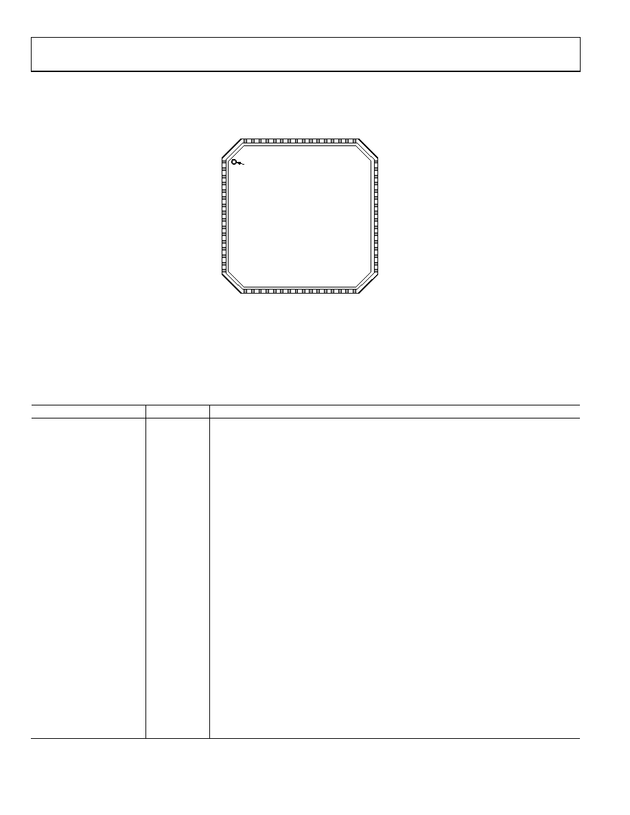
Figure 5. Pin Configuration
Table 8. Pin Function Description
Pin No.
Mnemonic
Description
0
GND
Exposed paddle is the only ground connection for the chip. Must be connected to PCB AGND.
1, 2
CLK+, CLK
Differential Encode Clock. PECL, LVDS, or 1.8 V CMOS inputs.
3
SYNC
Digital Input. SYNC input to clock divider. 30 kΩ internal pull-down.
4, 5, 6, 7, 8, 9, 25, 26, 27,
29, 30, 31
NC
Do Not Connect.
10, 19, 28, 37
DRVDD
Digital Output Driver Supply (1.8 V to 3.3 V).
11 to 18, 20, 21
D0B to D9B
Channel B Digital Outputs. D9B = MSB.
22
ORB
Channel B Out-of-Range Digital Output.
23
DCOB
Channel B Data Clock Digital Output.
24
DCOA
Channel A Data Clock Digital Output.
32 to 36, 38 to 42
D0A to D9A
Channel A Digital Outputs. D9A = MSB.
43
ORA
Channel A Out-of-Range Digital Output.
44
SDIO/DCS
SPI Data Input/Output (SDIO). Bidirectional SPI Data I/O in SPI mode. 30 kΩ internal pull-
down in SPI mode.
Duty Cycle Stabilizer (DCS). Static enable input for duty cycle stabilizer in non-SPI mode.
30 kΩ internal pull-up in non-SPI (DCS) mode.
45
SCLK/DFS
SPI Clock (SCLK) Input in SPI mode. 30 kΩ internal pull-down.
Data Format Select (DFS). Static control of data output format in non-SPI mode. 30 kΩ internal
pull-down.
DFS high = twos complement output.
DFS low = offset binary output.
46
CSB
SPI Chip Select. Active low enable; 30 kΩ internal pull-up.
47
OEB
Digital Input. Enable Channel A and Channel B digital outputs if low, three-state outputs if
high. 30 kΩ internal pull-down.
48
PDWN
Digital Input. 30 kΩ internal pull-down.
PDWN high = power-down device.
PDWN low = run device, normal operation.
相关PDF资料 |
PDF描述 |
|---|---|
| MS3106E24-9P | CONN PLUG 2POS STRAIGHT W/PINS |
| MS3106E22-22PY | CONN PLUG 4POS STRAIGHT W/PINS |
| CS5560-ISZR | IC ADC 24BIT DELTA-SIGMA 24-SSOP |
| AD7739BRUZ-REEL7 | IC ADC 24BIT 8CH SIG-DEL 24TSSOP |
| AD9223ARSZ-REEL | IC ADC 12BIT 3.0MSPS 28SSOP |
相关代理商/技术参数 |
参数描述 |
|---|---|
| AD9204BCPZRL7-80 | 功能描述:IC ADC 10BIT 80MSPS 64LFCSP RoHS:是 类别:集成电路 (IC) >> 数据采集 - 模数转换器 系列:- 标准包装:1,000 系列:- 位数:12 采样率(每秒):300k 数据接口:并联 转换器数目:1 功率耗散(最大):75mW 电压电源:单电源 工作温度:0°C ~ 70°C 安装类型:表面贴装 封装/外壳:24-SOIC(0.295",7.50mm 宽) 供应商设备封装:24-SOIC 包装:带卷 (TR) 输入数目和类型:1 个单端,单极;1 个单端,双极 |
| AD9208BBPZRL-3000 | |
| AD9211 | 制造商:AD 制造商全称:Analog Devices 功能描述:10-Bit, 200 MSPS/250 MSPS/300 MSPS, 1.8 V Analog-to-Digital Converter |
| AD9211_07 | 制造商:AD 制造商全称:Analog Devices 功能描述:10-Bit, 200 MSPS/250 MSPS/300 MSPS, 1.8 V Analog-to-Digital Converter |
| AD9211-170EB | 制造商:AD 制造商全称:Analog Devices 功能描述:10-Bit, 170/200/250 MSPS 1.8 V A/D Converter |
发布紧急采购,3分钟左右您将得到回复。