- 您现在的位置:买卖IC网 > PDF目录10163 > AD9225ARSRL (Analog Devices Inc)IC ADC 12BIT 25MSPS 28-SSOP PDF资料下载
参数资料
| 型号: | AD9225ARSRL |
| 厂商: | Analog Devices Inc |
| 文件页数: | 1/25页 |
| 文件大小: | 0K |
| 描述: | IC ADC 12BIT 25MSPS 28-SSOP |
| 标准包装: | 1,500 |
| 位数: | 12 |
| 采样率(每秒): | 25M |
| 数据接口: | 并联 |
| 转换器数目: | 7 |
| 功率耗散(最大): | 373mW |
| 电压电源: | 单电源 |
| 工作温度: | -40°C ~ 85°C |
| 安装类型: | 表面贴装 |
| 封装/外壳: | 28-SSOP(0.209",5.30mm 宽) |
| 供应商设备封装: | 28-SSOP |
| 包装: | 带卷 (TR) |
| 输入数目和类型: | 2 个单端,双极;1 个差分,单极 |
Information furnished by Analog Devices is believed to be accurate and
reliable. However, no responsibility is assumed by Analog Devices for its
use, nor for any infringements of patents or other rights of third parties that
may result from its use. No license is granted by implication or otherwise
under any patent or patent rights of Analog Devices. Trademarks and
registered trademarks are the property of their respective owners.
One Technology Way, P.O. Box 9106, Norwood, MA 02062-9106, U.S.A.
Tel: 781/329-4700
Fax:
Analog Devices, Inc. All rights reserved.
AD9225
Complete 12-Bit, 25 MSPS
Monolithic A/D Converter
FEATURES
Monolithic 12-Bit, 25 MSPS ADC
Low Power Dissipation: 280 mW
Single 5 V Supply
No Missing Codes Guaranteed
Differential Nonlinearity Error:
0.4 LSB
Complete On-Chip Sample-and-Hold Amplifier and
Voltage Reference
Signal-to-Noise and Distortion Ratio: 71 dB
Spurious-Free Dynamic Range: –85 dB
Out-of-Range Indicator
Straight Binary Output Data
28-Lead SOIC
28-Lead SSOP
Compatible with 3 V Logic
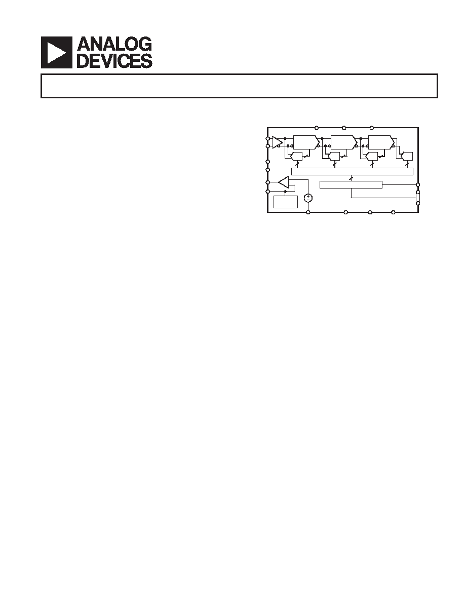
FUNCTIONAL BLOCK DIAGRAM
VINA
CAPT
CAPB
SENSE
OTR
BIT 1
(MSB)
BIT 12
(LSB)
VREF
DRVSS
AVSS
CML
AD9225
SHA
DIGITAL CORRECTION LOGIC
OUTPUT BUFFERS
VINB
1V
REFCOM
5
3
4
12
DRVDD
AVDD
CLK
MODE
SELECT
MDAC3
GAIN = 4
MDAC2
GAIN = 4
MDAC1
GAIN = 16
ADC
GENERAL DESCRIPTION
The AD9225 is a monolithic, single-supply, 12-bit, 25 MSPS
analog-to-digital converter with an on-chip, high performance
sample-and-hold amplifier and voltage reference. The AD9225
uses a multistage differential pipelined architecture with output
error correction logic to provide 12-bit accuracy at 25 MSPS
data rates, and guarantees no missing codes over the full operat-
ing temperature range.
The AD9225 combines a low cost, high speed CMOS process
and a novel architecture to achieve the resolution and speed of
existing bipolar implementations at a fraction of the power
consumption and cost.
The input of the AD9225 allows for easy interfacing to both
imaging and communications systems. With the device’s truly
differential input structure, the user can select a variety of input
ranges and offsets, including single-ended applications. The
dynamic performance is excellent.
The sample-and-hold amplifier (SHA) is well suited for both
multiplexed systems that switch full-scale voltage levels in succes-
sive channels and sampling single-channel inputs at frequencies
up to and well beyond the Nyquist rate.
The AD9225’s wideband input, combined with the power and
cost savings over previously available monolithics, suits applica-
tions in communications, imaging, and medical ultrasound.
The AD9225 has an on-board programmable reference. An
external reference can also be chosen to suit the dc accuracy
and temperature drift requirements of an application.
A single clock input is used to control all internal conversion
cycles. The digital output data is presented in straight binary
output format. An out-of-range signal indicates an overflow
condition that can be used with the most significant bit to deter-
mine low or high overflow.
PRODUCT HIGHLIGHTS
The AD9225 is fabricated on a very cost effective CMOS pro-
cess. High speed precision analog circuits are combined with
high density logic circuits.
The AD9225 offers a complete, single-chip sampling, 12-bit,
25 MSPS analog-to-digital conversion function in 28-lead
SOIC and SSOP packages.
Low Power—The AD9225 at 280 mW consumes a fraction of
the power presently available in monolithic solutions.
On-Board Sample-and-Hold Amplifier (SHA)—The versa-
tile SHA input can be configured for either single-ended or
differential inputs.
Out-of-Range (OTR)—The OTR output bit indicates when
the input signal is beyond the AD9225’s input range.
Single Supply—The AD9225 uses a single 5 V power supply,
simplifying system power supply design. It also features a sepa-
rate digital driven supply line to accommodate 3 V and 5 V logic
families.
Pin Compatibility—The AD9225 is pin compatible with the
AD9220, AD9221, AD9223, and AD9224 ADCs.
Rev. C
781/461-3113 1998-2011
相关PDF资料 |
PDF描述 |
|---|---|
| SP26LV432CN-L | IC DVR RS422 DIFF QUAD 16NSOIC |
| VI-B3H-MW-F3 | CONVERTER MOD DC/DC 52V 100W |
| VE-25P-IU-F4 | CONVERTER MOD DC/DC 13.8V 200W |
| MS27467T19B11PB | CONN PLUG 11POS STRAIGHT W/PINS |
| VE-25P-IU-F3 | CONVERTER MOD DC/DC 13.8V 200W |
相关代理商/技术参数 |
参数描述 |
|---|---|
| AD9225ARSZ | 功能描述:IC ADC 12BIT 25MSPS 28-SSOP RoHS:是 类别:集成电路 (IC) >> 数据采集 - 模数转换器 系列:- 标准包装:1 系列:microPOWER™ 位数:8 采样率(每秒):1M 数据接口:串行,SPI? 转换器数目:1 功率耗散(最大):- 电压电源:模拟和数字 工作温度:-40°C ~ 125°C 安装类型:表面贴装 封装/外壳:24-VFQFN 裸露焊盘 供应商设备封装:24-VQFN 裸露焊盘(4x4) 包装:Digi-Reel® 输入数目和类型:8 个单端,单极 产品目录页面:892 (CN2011-ZH PDF) 其它名称:296-25851-6 |
| AD9225ARSZ | 制造商:Analog Devices 功能描述:IC 制造商:Analog Devices 功能描述:IC, ADC, 12BIT, 25MSPS, SSOP-28 |
| AD9225ARSZRL | 功能描述:IC ADC 12BIT 25MSPS 28SSOP RoHS:是 类别:集成电路 (IC) >> 数据采集 - 模数转换器 系列:- 标准包装:1,000 系列:- 位数:12 采样率(每秒):300k 数据接口:并联 转换器数目:1 功率耗散(最大):75mW 电压电源:单电源 工作温度:0°C ~ 70°C 安装类型:表面贴装 封装/外壳:24-SOIC(0.295",7.50mm 宽) 供应商设备封装:24-SOIC 包装:带卷 (TR) 输入数目和类型:1 个单端,单极;1 个单端,双极 |
| AD9225ARZ | 功能描述:IC ADC 12BIT 25MSPS 28-SOIC RoHS:是 类别:集成电路 (IC) >> 数据采集 - 模数转换器 系列:- 标准包装:1 系列:microPOWER™ 位数:8 采样率(每秒):1M 数据接口:串行,SPI? 转换器数目:1 功率耗散(最大):- 电压电源:模拟和数字 工作温度:-40°C ~ 125°C 安装类型:表面贴装 封装/外壳:24-VFQFN 裸露焊盘 供应商设备封装:24-VQFN 裸露焊盘(4x4) 包装:Digi-Reel® 输入数目和类型:8 个单端,单极 产品目录页面:892 (CN2011-ZH PDF) 其它名称:296-25851-6 |
| AD9225ARZRL | 功能描述:IC ADC 12BIT 25MSPS 28SOIC RoHS:是 类别:集成电路 (IC) >> 数据采集 - 模数转换器 系列:- 标准包装:1,000 系列:- 位数:12 采样率(每秒):300k 数据接口:并联 转换器数目:1 功率耗散(最大):75mW 电压电源:单电源 工作温度:0°C ~ 70°C 安装类型:表面贴装 封装/外壳:24-SOIC(0.295",7.50mm 宽) 供应商设备封装:24-SOIC 包装:带卷 (TR) 输入数目和类型:1 个单端,单极;1 个单端,双极 |
发布紧急采购,3分钟左右您将得到回复。