- 您现在的位置:买卖IC网 > PDF目录10163 > AD9225ARSRL (Analog Devices Inc)IC ADC 12BIT 25MSPS 28-SSOP PDF资料下载
参数资料
| 型号: | AD9225ARSRL |
| 厂商: | Analog Devices Inc |
| 文件页数: | 5/25页 |
| 文件大小: | 0K |
| 描述: | IC ADC 12BIT 25MSPS 28-SSOP |
| 标准包装: | 1,500 |
| 位数: | 12 |
| 采样率(每秒): | 25M |
| 数据接口: | 并联 |
| 转换器数目: | 7 |
| 功率耗散(最大): | 373mW |
| 电压电源: | 单电源 |
| 工作温度: | -40°C ~ 85°C |
| 安装类型: | 表面贴装 |
| 封装/外壳: | 28-SSOP(0.209",5.30mm 宽) |
| 供应商设备封装: | 28-SSOP |
| 包装: | 带卷 (TR) |
| 输入数目和类型: | 2 个单端,双极;1 个差分,单极 |
AD9225
–13–
10 F
VINA
VINB
SENSE
AD9225
0.1 F
RS
+V
–V
RS
VREF
4V
0V
U1
2.0V
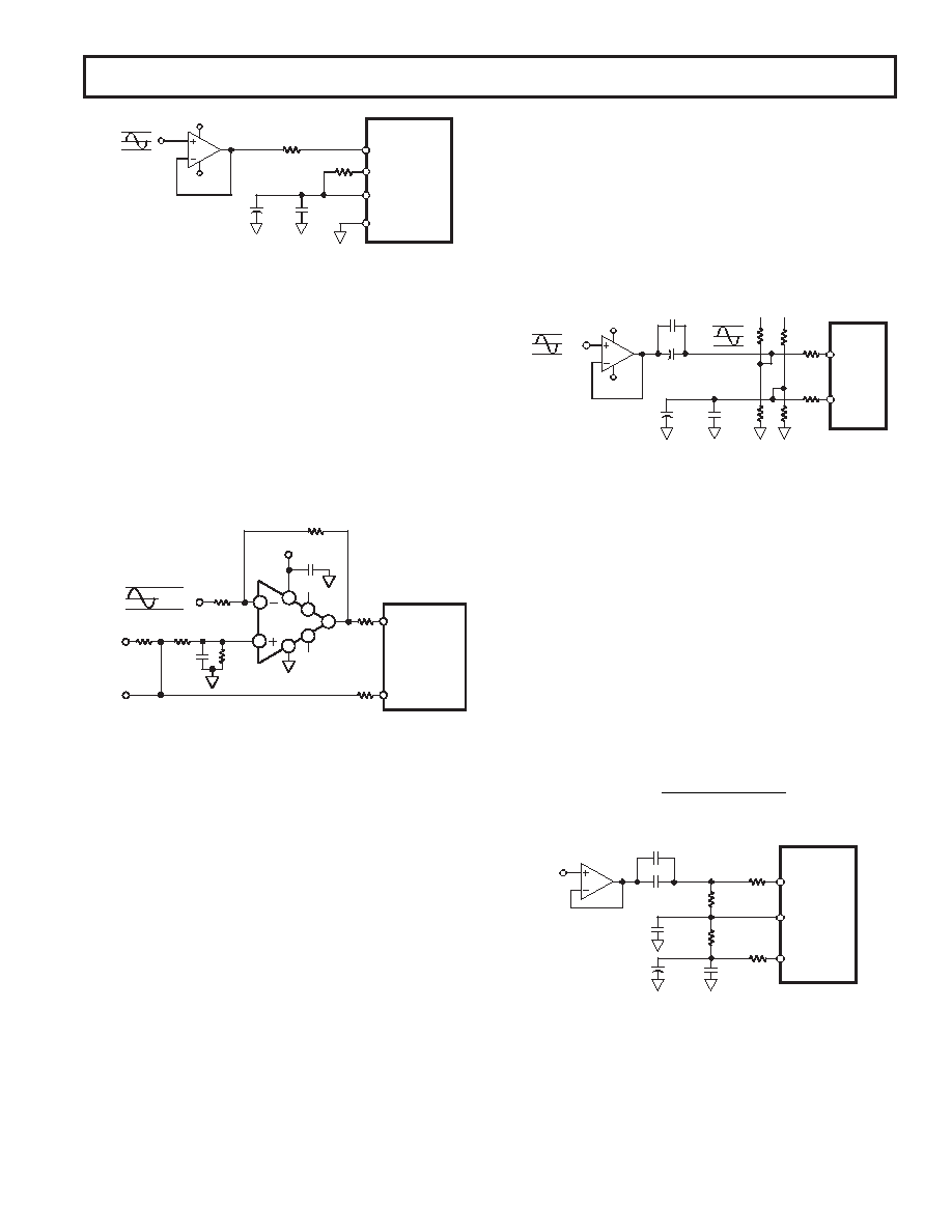
Figure 8. Single-Ended AD9225 Op Amp Drive Circuit
Op Amp with DC Level Shifting
Figure 9 shows a dc-coupled level shifting circuit employing an op
amp, A1, to sum the input signal with the desired dc set. Configur-
ing the op amp in the inverting mode with the given resistor values
results in an ac signal gain of –1. If the signal inversion is undesir-
able, interchange the VINA and VINB connections to re-establish
the original signal polarity. The dc voltage at VREF sets the
common-mode voltage of the AD9225. For example, when
VREF = 2.0 V, the input level from the op amp will also be cen-
tered around 2.0 V. The use of ratio matched, thin-film resistor
networks will minimize gain and offset errors. Also, an optional
pull-up resistor, RP, may be used to reduce the output load on
VREF to less than its 1 mA maximum.
0VDC
+VREF
–VREF
VINA
VINB
AD9225
0.1 F
500 *
0.1 F
500 *
7
1
2
3
4
5
A1
6
NC
+VCC
500 *
RS
VREF
500 *
RS
RP**
+V
*
OPTIONAL RESISTOR NETWORK-OHMTEK ORNA500D
**
OPTIONAL PULL-UP RESISTOR WHEN USING INTERNAL REFERENCE
Figure 9. Single-Ended Input with DC-Coupled Level Shift
AC COUPLING AND INTERFACE ISSUES
For applications where ac coupling is appropriate, the op amp
output can be easily level-shifted via a coupling capacitor. This has
the advantage of allowing the op amp common-mode level to be
symmetrically biased to its midsupply level (i.e., (VCC + VEE)/2).
Op amps that operate symmetrically with respect to their power
supplies typically provide the best ac performance as well as great-
est input/output span. Various high speed/performance amplifiers
which are restricted to +5 V/–5 V operation and/or specified for
+5 V single-supply operation can be easily configured for the 4 V
or 2 V input span of the AD9225. Note that differential trans-
former coupling, which is another form of ac coupling, should be
considered for optimum ac performance.
Simple AC Interface
Figure 10 shows a typical example of an ac-coupled, single-ended
configuration. The bias voltage shifts the bipolar, ground-refer-
enced input signal to approximately AVDD/2. The value for C1
and C2 will depend on the size of the resistor, R. The capacitors,
C1 and C2, are a 0.1
mF ceramic and 10 mF tantalum capacitor in
parallel to achieve a low cutoff frequency while maintaining a low
impedance over a wide frequency range. The combination of the
capacitor and the resistor form a high-pass filter with a high-pass –
3 dB frequency determined by the equation
f–3 dB = 1/(2
R (C1 + C2))
The low impedance VREF voltage source biases both the VINB
input and provides the bias voltage for the VINA input. Figure 10
shows the VREF configured for 2.0 V thus the input range of the
ADC is 0 V to 4 V. Other input ranges could be selected by chang-
ing VREF.
VINA
VINB
AD9225
+5V
–5V
RS
0V
+2V
–2V
VIN
C1
10 F
RS
AD9631
+V
C2
0.1 F
10 F
0.1 F
0.5
2.5
4.5
R
Figure 10. AC-Coupled Input
Alternative AC Interface
Figure 11 shows a flexible ac-coupled circuit that can be config-
ured for different input spans. Since the common-mode voltage of
VINA and VINB are biased to midsupply independent of VREF,
VREF can be pin strapped or reconfigured to achieve input spans
between 2 V and 4 V p-p. The AD9225’s CMRR along with the
symmetrical coupling R-C networks will reject both power supply
variations and noise. The resistors, R, establish the common-mode
voltage. They may have a high value (e.g., 5 k
W) to minimize
power consumption and establish a low cutoff frequency. The
capacitors, C1 and C2, are typically a 0.1
mF ceramic and 10 mF
tantalum capacitor in parallel to achieve a low cutoff frequency
while maintaining a low impedance over a wide frequency range.
RS isolates the buffer amplifier from the ADC input. The optimum
performance is achieved when VINA and VINB are driven via
symmetrical networks. The f–3 dB point can be approximated by
the equation
f –3dB
=
1
2
p6K +(C1+C2)
VINA
VINB
AD9225
1k
RS
VIN
C2
0.1 F
RS
VCM
1k
C2
0.1 F
C1
10 F
C1
10 F
C3
0.1 F
Figure 11. AC-Coupled Input-Flexible Input Span,
VCM = 2.5 V
Rev. C
相关PDF资料 |
PDF描述 |
|---|---|
| SP26LV432CN-L | IC DVR RS422 DIFF QUAD 16NSOIC |
| VI-B3H-MW-F3 | CONVERTER MOD DC/DC 52V 100W |
| VE-25P-IU-F4 | CONVERTER MOD DC/DC 13.8V 200W |
| MS27467T19B11PB | CONN PLUG 11POS STRAIGHT W/PINS |
| VE-25P-IU-F3 | CONVERTER MOD DC/DC 13.8V 200W |
相关代理商/技术参数 |
参数描述 |
|---|---|
| AD9225ARSZ | 功能描述:IC ADC 12BIT 25MSPS 28-SSOP RoHS:是 类别:集成电路 (IC) >> 数据采集 - 模数转换器 系列:- 标准包装:1 系列:microPOWER™ 位数:8 采样率(每秒):1M 数据接口:串行,SPI? 转换器数目:1 功率耗散(最大):- 电压电源:模拟和数字 工作温度:-40°C ~ 125°C 安装类型:表面贴装 封装/外壳:24-VFQFN 裸露焊盘 供应商设备封装:24-VQFN 裸露焊盘(4x4) 包装:Digi-Reel® 输入数目和类型:8 个单端,单极 产品目录页面:892 (CN2011-ZH PDF) 其它名称:296-25851-6 |
| AD9225ARSZ | 制造商:Analog Devices 功能描述:IC 制造商:Analog Devices 功能描述:IC, ADC, 12BIT, 25MSPS, SSOP-28 |
| AD9225ARSZRL | 功能描述:IC ADC 12BIT 25MSPS 28SSOP RoHS:是 类别:集成电路 (IC) >> 数据采集 - 模数转换器 系列:- 标准包装:1,000 系列:- 位数:12 采样率(每秒):300k 数据接口:并联 转换器数目:1 功率耗散(最大):75mW 电压电源:单电源 工作温度:0°C ~ 70°C 安装类型:表面贴装 封装/外壳:24-SOIC(0.295",7.50mm 宽) 供应商设备封装:24-SOIC 包装:带卷 (TR) 输入数目和类型:1 个单端,单极;1 个单端,双极 |
| AD9225ARZ | 功能描述:IC ADC 12BIT 25MSPS 28-SOIC RoHS:是 类别:集成电路 (IC) >> 数据采集 - 模数转换器 系列:- 标准包装:1 系列:microPOWER™ 位数:8 采样率(每秒):1M 数据接口:串行,SPI? 转换器数目:1 功率耗散(最大):- 电压电源:模拟和数字 工作温度:-40°C ~ 125°C 安装类型:表面贴装 封装/外壳:24-VFQFN 裸露焊盘 供应商设备封装:24-VQFN 裸露焊盘(4x4) 包装:Digi-Reel® 输入数目和类型:8 个单端,单极 产品目录页面:892 (CN2011-ZH PDF) 其它名称:296-25851-6 |
| AD9225ARZRL | 功能描述:IC ADC 12BIT 25MSPS 28SOIC RoHS:是 类别:集成电路 (IC) >> 数据采集 - 模数转换器 系列:- 标准包装:1,000 系列:- 位数:12 采样率(每秒):300k 数据接口:并联 转换器数目:1 功率耗散(最大):75mW 电压电源:单电源 工作温度:0°C ~ 70°C 安装类型:表面贴装 封装/外壳:24-SOIC(0.295",7.50mm 宽) 供应商设备封装:24-SOIC 包装:带卷 (TR) 输入数目和类型:1 个单端,单极;1 个单端,双极 |
发布紧急采购,3分钟左右您将得到回复。