- 您现在的位置:买卖IC网 > PDF目录10163 > AD9225ARSRL (Analog Devices Inc)IC ADC 12BIT 25MSPS 28-SSOP PDF资料下载
参数资料
| 型号: | AD9225ARSRL |
| 厂商: | Analog Devices Inc |
| 文件页数: | 25/25页 |
| 文件大小: | 0K |
| 描述: | IC ADC 12BIT 25MSPS 28-SSOP |
| 标准包装: | 1,500 |
| 位数: | 12 |
| 采样率(每秒): | 25M |
| 数据接口: | 并联 |
| 转换器数目: | 7 |
| 功率耗散(最大): | 373mW |
| 电压电源: | 单电源 |
| 工作温度: | -40°C ~ 85°C |
| 安装类型: | 表面贴装 |
| 封装/外壳: | 28-SSOP(0.209",5.30mm 宽) |
| 供应商设备封装: | 28-SSOP |
| 包装: | 带卷 (TR) |
| 输入数目和类型: | 2 个单端,双极;1 个差分,单极 |
AD9225
–9–
Due to the high degree of symmetry within the SHA topology, a
significant improvement in distortion performance for differen-
tial input signals with frequencies up to and beyond Nyquist can
be realized. This inherent symmetry provides excellent cancella-
tion of both common-mode distortion and noise. Also, the
required input signal voltage span is reduced by a half, which
further reduces the degree of RON modulation and its effects
on distortion.
The optimum noise and dc linearity performance for either
differential or single-ended inputs is achieved with the largest
input signal voltage span (i.e., 4 V input span) and matched
input impedance for VINA and VINB. Only a slight degrada-
tion in dc linearity performance exists between the 2 V and 4 V
input spans.
Referring to Figure 3, the differential SHA is implemented
using a switched capacitor topology. Its input impedance and its
switching effects on the input drive source should be considered
in order to maximize the converter’s performance. The combi-
nation of the pin capacitance, CPIN, parasitic capacitance, CPAR,
and the sampling capacitance, CS, is typically less than 5 pF.
When the SHA goes into track mode, the input source must
charge or discharge the voltage stored on CS to the new input
voltage. This action of charging and discharging CS, averaged
over a period of time and for a given sampling frequency, fS,
makes the input impedance appear to have a benign resistive
component. However, if this action is analyzed within a sampling
period (i.e., T = 1/fS), the input impedance is dynamic and
therefore certain precautions on the input drive source should
be observed.
The resistive component to the input impedance can be com-
puted by calculating the average charge that gets drawn by CH
from the input drive source. It can be shown that if CS is al-
lowed to fully charge up to the input voltage before switches
QS1 are opened, then the average current into the input would
be the same as it would if there were a resistor of 1/(CS fS) Ohms
connected between the inputs. This means that the input im-
pedance is inversely proportional to the converter’s sample
rate. Since CS is only 5 pF, this resistive component is typically
much larger than that of the drive source (i.e., 8 k
W at fS =
25 MSPS).
The SHA’s input impedance over a sampling period appears as
a dynamic input impedance to the input drive source. When the
SHA goes into the track mode, the input source ideally should
provide the charging current through RON of switch QS1 in an
exponential manner. The requirement of exponential charging
means that the most common input source, an op amp, must
exhibit a source impedance that is both low and resistive up to
and beyond the sampling frequency.
The output impedance of an op amp can be modeled with a
series inductor and resistor. When a capacitive load is switched
onto the output of the op amp, the output will momentarily
drop due to its effective output impedance. As the output recov-
ers, ringing may occur. To remedy the situation, a series resistor
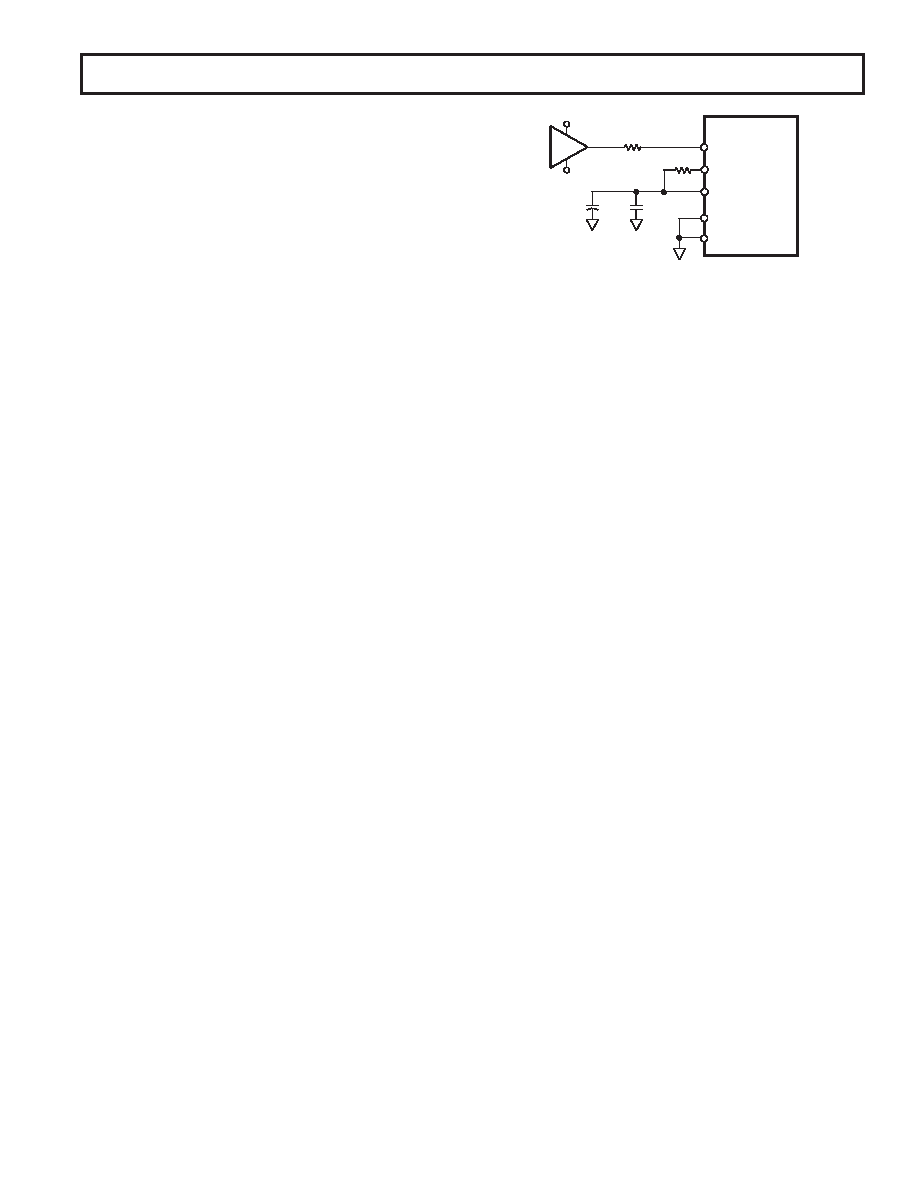
can be inserted between the op amp and the SHA input as
shown in Figure 4. The series resistance helps isolate the op
amp from the switched capacitor load.
10 F
VINA
VINB
SENSE
AD9225
0.1 F
RS
VCC
VEE
RS
VREF
REFCOM
Figure 4. Series Resistor Isolates Switched Capacitor
SHA Input from Op Amp. Matching Resistors Improve
SNR Performance.
The optimum size of this resistor is dependent on several fac-
tors, which include the ADC sampling rate, the selected op
amp, and the particular application. In most applications, a
30
W to 100 W resistor is sufficient. However, some applica-
tions may require a larger resistor value to reduce the noise
bandwidth or possibly to limit the fault current in an overvolt-
age condition. Other applications may require a larger resistor
value as part of an antialiasing filter. In any case, since the THD
performance is dependent on the series resistance and the above
mentioned factors, optimizing this resistor value for a given
application is encouraged.
The source impedance driving VINA and VINB should be
matched. Failure to provide that matching will result in degra-
dation of the AD9225’s superb SNR, THD, and SFDR.
For noise sensitive applications, the very high bandwidth of the
AD9225 may be detrimental. The addition of a series resistor
and/or shunt capacitor can help limit the wideband noise at the
ADC’s input by forming a low-pass filter. Note, however, that
the combination of this series resistance with the equivalent
input capacitance of the AD9225 should be evaluated for
those time domain applications that are sensitive to the input
signal’s absolute settling time. In applications where harmonic
distortion is not a primary concern, the series resistance may be
selected in combination with the SHA’s nominal 10 pF of input
capacitance to set the filter’s 3 dB cutoff frequency.
A better method of reducing the noise bandwidth, while possi-
bly establishing a real pole for an antialiasing filter, is to add
some additional shunt capacitance between the input (i.e.,
VINA and/or VINB) and analog ground. Since this additional
shunt capacitance combines with the equivalent input capaci-
tance of the AD9225, a lower series resistance can be selected to
establish the filter’s cutoff frequency while not degrading the
distortion performance of the device. The shunt capacitance
also acts like a charge reservoir, sinking or sourcing the addi-
tional charge required by the hold capacitor, CH, and further
reducing current transients seen at the op amp’s output.
The effect of this increased capacitive load on the op amp driv-
ing the AD9225 should be evaluated. To optimize performance
when noise is the primary consideration, increase the shunt
capacitance as much as the transient response of the input signal
will allow. Increasing the capacitance too much may adversely
affect the op amp’s settling time, frequency response, and dis-
tortion performance.
Rev. C
相关PDF资料 |
PDF描述 |
|---|---|
| SP26LV432CN-L | IC DVR RS422 DIFF QUAD 16NSOIC |
| VI-B3H-MW-F3 | CONVERTER MOD DC/DC 52V 100W |
| VE-25P-IU-F4 | CONVERTER MOD DC/DC 13.8V 200W |
| MS27467T19B11PB | CONN PLUG 11POS STRAIGHT W/PINS |
| VE-25P-IU-F3 | CONVERTER MOD DC/DC 13.8V 200W |
相关代理商/技术参数 |
参数描述 |
|---|---|
| AD9225ARSZ | 功能描述:IC ADC 12BIT 25MSPS 28-SSOP RoHS:是 类别:集成电路 (IC) >> 数据采集 - 模数转换器 系列:- 标准包装:1 系列:microPOWER™ 位数:8 采样率(每秒):1M 数据接口:串行,SPI? 转换器数目:1 功率耗散(最大):- 电压电源:模拟和数字 工作温度:-40°C ~ 125°C 安装类型:表面贴装 封装/外壳:24-VFQFN 裸露焊盘 供应商设备封装:24-VQFN 裸露焊盘(4x4) 包装:Digi-Reel® 输入数目和类型:8 个单端,单极 产品目录页面:892 (CN2011-ZH PDF) 其它名称:296-25851-6 |
| AD9225ARSZ | 制造商:Analog Devices 功能描述:IC 制造商:Analog Devices 功能描述:IC, ADC, 12BIT, 25MSPS, SSOP-28 |
| AD9225ARSZRL | 功能描述:IC ADC 12BIT 25MSPS 28SSOP RoHS:是 类别:集成电路 (IC) >> 数据采集 - 模数转换器 系列:- 标准包装:1,000 系列:- 位数:12 采样率(每秒):300k 数据接口:并联 转换器数目:1 功率耗散(最大):75mW 电压电源:单电源 工作温度:0°C ~ 70°C 安装类型:表面贴装 封装/外壳:24-SOIC(0.295",7.50mm 宽) 供应商设备封装:24-SOIC 包装:带卷 (TR) 输入数目和类型:1 个单端,单极;1 个单端,双极 |
| AD9225ARZ | 功能描述:IC ADC 12BIT 25MSPS 28-SOIC RoHS:是 类别:集成电路 (IC) >> 数据采集 - 模数转换器 系列:- 标准包装:1 系列:microPOWER™ 位数:8 采样率(每秒):1M 数据接口:串行,SPI? 转换器数目:1 功率耗散(最大):- 电压电源:模拟和数字 工作温度:-40°C ~ 125°C 安装类型:表面贴装 封装/外壳:24-VFQFN 裸露焊盘 供应商设备封装:24-VQFN 裸露焊盘(4x4) 包装:Digi-Reel® 输入数目和类型:8 个单端,单极 产品目录页面:892 (CN2011-ZH PDF) 其它名称:296-25851-6 |
| AD9225ARZRL | 功能描述:IC ADC 12BIT 25MSPS 28SOIC RoHS:是 类别:集成电路 (IC) >> 数据采集 - 模数转换器 系列:- 标准包装:1,000 系列:- 位数:12 采样率(每秒):300k 数据接口:并联 转换器数目:1 功率耗散(最大):75mW 电压电源:单电源 工作温度:0°C ~ 70°C 安装类型:表面贴装 封装/外壳:24-SOIC(0.295",7.50mm 宽) 供应商设备封装:24-SOIC 包装:带卷 (TR) 输入数目和类型:1 个单端,单极;1 个单端,双极 |
发布紧急采购,3分钟左右您将得到回复。