- 您现在的位置:买卖IC网 > PDF目录10514 > AD9229ABCPZ-65 (Analog Devices Inc)IC ADC 12BIT SRL 65MSPS 48LFCSP PDF资料下载
参数资料
| 型号: | AD9229ABCPZ-65 |
| 厂商: | Analog Devices Inc |
| 文件页数: | 10/40页 |
| 文件大小: | 0K |
| 描述: | IC ADC 12BIT SRL 65MSPS 48LFCSP |
| 标准包装: | 1 |
| 位数: | 12 |
| 采样率(每秒): | 65M |
| 数据接口: | 串行 |
| 转换器数目: | 4 |
| 功率耗散(最大): | 1.47W |
| 电压电源: | 模拟和数字 |
| 工作温度: | -40°C ~ 85°C |
| 安装类型: | 表面贴装 |
| 封装/外壳: | 48-VFQFN 裸露焊盘,CSP |
| 供应商设备封装: | 48-LFCSP-VQ(7x7) |
| 包装: | 托盘 |
| 输入数目和类型: | 8 个单端,单极;4 个差分,单极 |
第1页第2页第3页第4页第5页第6页第7页第8页第9页当前第10页第11页第12页第13页第14页第15页第16页第17页第18页第19页第20页第21页第22页第23页第24页第25页第26页第27页第28页第29页第30页第31页第32页第33页第34页第35页第36页第37页第38页第39页第40页
AD9229
Rev. B | Page 18 of 40
THEORY OF OPERATION
The AD9229 architecture consists of a front-end switched capa-
citor sample-and-hold amplifier (SHA) followed by a pipelined
ADC. The pipelined ADC is divided into three sections: a 4-bit
first stage followed by eight 1.5-bit stages and a final 3-bit flash.
Each stage provides sufficient overlap to correct for flash errors
in the preceding stages. The quantized outputs from each stage
are combined into a final 12-bit result in the digital correction
logic. The pipelined architecture permits the first stage to
operate on a new input sample while the remaining stages
operate on preceding samples. Sampling occurs on the rising
edge of the clock.
Each stage of the pipeline, excluding the last, consists of a low
resolution flash ADC connected to a switched capacitor DAC
and interstage residue amplifier (MDAC). The residue amplifier
magnifies the difference between the reconstructed DAC output
and the flash input for the next stage in the pipeline. One bit of
redundancy is used in each stage to facilitate digital correction
of flash errors. The last stage simply consists of a flash ADC.
The input stage contains a differential SHA that can be config-
ured as ac- or dc-coupled in differential or single-ended modes.
The output staging block aligns the data, carries out the error
correction, and passes the data to the output buffers. The data is
then serialized and aligned to the frame and output clock.
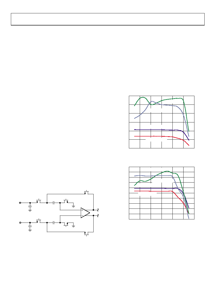
ANALOG INPUT CONSIDERATIONS
The analog input to the AD9229 is a differential switched-
capacitor SHA that has been designed for optimum perfor-
mance while processing a differential input signal. The SHA
input can support a wide common-mode range and maintain
excellent performance. An input common-mode voltage of
midsupply minimizes signal-dependent errors and provides
optimum performance.
04418-
029
H
VIN+
VIN–
CPAR
S
Figure 34. Switched-Capacitor SHA Input
The clock signal alternately switches the SHA between sample
mode and hold mode (see Figure 34). When the SHA is
switched into sample mode, the signal source must be capable
of charging the sample capacitors and settling within one-half
of a clock cycle. A small resistor in series with each input can
help reduce the peak transient current required from the output
stage of the driving source. Also, a small shunt capacitor can
be placed across the inputs to provide dynamic charging
currents. This passive network creates a low-pass filter at the
ADC’s input; therefore, the precise values are dependent on
the application.
The analog inputs of the AD9229 are not internally dc-biased.
In ac-coupled applications, the user must provide this bias
externally. For optimum performance, set the device so that
VCM = AVDD/2; however, the device can function over a wider
range with reasonable performance (see Figure 35 and Figure 36).
ANALOG INPUT COMMON-MODE VOLTAGE (V)
S
NR/S
F
DR
(dB)
90
85
75
80
65
60
70
0
2.5
3.0
2.0
1.5
1.0
0.5
04418-053
2V p-p, SFDR (dBc)
2V p-p, SNR (dB)
1V p-p, SNR (dB)
1V p-p, SFDR (dBc)
Figure 35. SNR/SFDR vs. Common-Mode Voltage, fIN = 2.4 MHz,
fSAMPLE = 65 MSPS
ANALOG INPUT COMMON-MODE VOLTAGE (V)
S
NR/S
F
DR
(dB)
90
65
55
60
45
40
50
85
75
80
70
0
2.5
3.0
2.0
1.5
1.0
0.5
04418-054
2V p-p, SFDR (dBc)
2V p-p, SNR (dB)
1V p-p, SNR (dB)
1V p-p, SFDR (dBc)
Figure 36. SNR/SFDR vs. Common-Mode Voltage, fIN = 30 MHz,
fSAMPLE = 65 MSPS
For best dynamic performance, the source impedances driving
VIN+ and VIN should be matched such that common-mode
settling errors are symmetrical. These errors are reduced by the
common-mode rejection of the ADC.
相关PDF资料 |
PDF描述 |
|---|---|
| VE-BT1-IV-F4 | CONVERTER MOD DC/DC 12V 150W |
| AD9260ASZ | IC ADC CMOS 16BIT OVRSAMP 44MQFP |
| MAX3041CUE+ | IC RS485/422 TRANS QUAD 16TSSOP |
| VE-BT1-IV-F3 | CONVERTER MOD DC/DC 12V 150W |
| EXP-0941/03/S | CONN BOX MNT 3POS IP68 W/SOCKETS |
相关代理商/技术参数 |
参数描述 |
|---|---|
| AD9229ABCPZRL7-50 | 功能描述:IC ADC 12BIT SRL 50MSPS 48LFCSP RoHS:是 类别:集成电路 (IC) >> 数据采集 - 模数转换器 系列:- 标准包装:1 系列:- 位数:14 采样率(每秒):83k 数据接口:串行,并联 转换器数目:1 功率耗散(最大):95mW 电压电源:双 ± 工作温度:0°C ~ 70°C 安装类型:通孔 封装/外壳:28-DIP(0.600",15.24mm) 供应商设备封装:28-PDIP 包装:管件 输入数目和类型:1 个单端,双极 |
| AD9229ABCPZRL7-65 | 功能描述:IC ADC 12BIT SRL 65MSPS 48LFCSP RoHS:是 类别:集成电路 (IC) >> 数据采集 - 模数转换器 系列:- 标准包装:1 系列:- 位数:14 采样率(每秒):83k 数据接口:串行,并联 转换器数目:1 功率耗散(最大):95mW 电压电源:双 ± 工作温度:0°C ~ 70°C 安装类型:通孔 封装/外壳:28-DIP(0.600",15.24mm) 供应商设备封装:28-PDIP 包装:管件 输入数目和类型:1 个单端,双极 |
| AD9229BBC-65 | 制造商:Analog Devices 功能描述:- Bulk |
| ad9229bcp-50 | 制造商:Analog Devices 功能描述: |
| AD9229BCP-65 | 制造商:Analog Devices 功能描述:- Bulk |
发布紧急采购,3分钟左右您将得到回复。