- 您现在的位置:买卖IC网 > PDF目录10514 > AD9229ABCPZ-65 (Analog Devices Inc)IC ADC 12BIT SRL 65MSPS 48LFCSP PDF资料下载
参数资料
| 型号: | AD9229ABCPZ-65 |
| 厂商: | Analog Devices Inc |
| 文件页数: | 17/40页 |
| 文件大小: | 0K |
| 描述: | IC ADC 12BIT SRL 65MSPS 48LFCSP |
| 标准包装: | 1 |
| 位数: | 12 |
| 采样率(每秒): | 65M |
| 数据接口: | 串行 |
| 转换器数目: | 4 |
| 功率耗散(最大): | 1.47W |
| 电压电源: | 模拟和数字 |
| 工作温度: | -40°C ~ 85°C |
| 安装类型: | 表面贴装 |
| 封装/外壳: | 48-VFQFN 裸露焊盘,CSP |
| 供应商设备封装: | 48-LFCSP-VQ(7x7) |
| 包装: | 托盘 |
| 输入数目和类型: | 8 个单端,单极;4 个差分,单极 |
第1页第2页第3页第4页第5页第6页第7页第8页第9页第10页第11页第12页第13页第14页第15页第16页当前第17页第18页第19页第20页第21页第22页第23页第24页第25页第26页第27页第28页第29页第30页第31页第32页第33页第34页第35页第36页第37页第38页第39页第40页
AD9229
Rev. B | Page 24 of 40
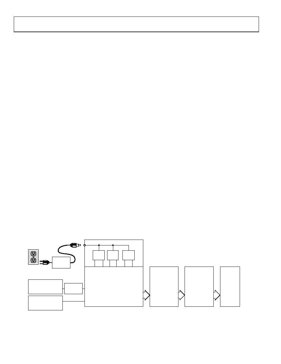
EVALUATION BOARD
The AD9229 evaluation board provides all of the support cir-
cuitry required to operate the ADC in its various modes and
configurations. The converter can be driven differentially
through a transformer (default) or through the AD8332 driver.
The ADC can also be driven in a single-ended fashion. Separate
power pins are provided to isolate the DUT from the AD8332
drive circuitry. Each input configuration can be selected by
proper connection of various jumpers (see Figure 48 to Figure 52).
Figure 47 shows the typical bench characterization setup used
to evaluate the ac performance of the AD9229. It is critical that
the signal sources used for the analog input and clock have very
low phase noise (<1 ps rms jitter) to realize the ultimate
performance of the converter. Proper filtering of the analog
input signal to remove harmonics and lower the integrated or
broadband noise at the input is also necessary to achieve the
specified noise performance.
plots that demonstrate the routing and grounding techniques
that should be applied at the system level.
POWER SUPPLIES
This evaluation board comes with a wall mountable switching
power supply that provides a 6 V, 2 A maximum output. Simply
connect the supply to the rated 100 V to 240 V ac wall outlet at
47 Hz to 63 Hz. The other end is a 2.1 mm inner diameter jack
that connects to the PCB at P503. Once on the PC board, the
6 V supply is fused and conditioned before connecting to three
low dropout linear regulators that supply the proper bias to each
of the various sections on the board.
When operating the evaluation board in a nondefault condition,
L504 to L506 can be removed to disconnect the switching
power supply. This enables the user to individually bias each
section of the board. Use P501 to connect a different supply for
each section. At least one 3.0 V supply is needed with a 1 A
current capability for AVDD_DUT and DRVDD_DUT;
however, it is recommended that separate supplies be used for
both analog and digital. To operate the evaluation board using
the VGA option, a separate 5.0 V analog supply is needed in
addition to the other 3.0 V supplies. The 5.0 V supply, or
AVDD_VGA, should have a 1 A current capability as well.
INPUT SIGNALS
When connecting the clock and analog source, use clean signal
generators with low phase noise, such as Rohde & Schwarz SMHU
or HP8644 signal generators or the equivalent. Use 1 m long,
shielded, RG-58, 50 Ω coaxial cable for making connections to
the evaluation board. Dial in the desired frequency and amplitude
within the ADC’s specifications tables. Typically, most ADI
evaluation boards can accept a ~2.8 V p-p or 13 dBm sine wave
input for the clock. When connecting the analog input source, it
is recommended to use a multipole, narrow-band band-pass
filter with 50 Ω terminations. ADI uses TTE, Allen Avionics,
and K&L types of band-pass filters. The filter should be
connected directly to the evaluation board if possible.
OUTPUT SIGNALS
The default setup uses the HSC-ADC-FPGA high speed
deserialization board, which deserializes the digital output data
and converts it to parallel CMOS. These two channels interface
directly with ADI’s standard dual-channel FIFO data capture
board (HSC-ADC-EVALA-DC). Two of the four channels can
then be evaluated at the same time. For more information on
channel settings on these boards and their optional settings,
visit www.analog.com/FIFO.
ROHDE & SCHWARZ,
SMHU,
2V p-p SIGNAL
SYNTHESIZER
ROHDE & SCHWARZ,
SMHU,
2V p-p SIGNAL
SYNTHESIZER
BAND-PASS
FILTER
XFMR
INPUT
CLK
CHA–CHD
12-BIT
SERIAL
LVDS
2 CH
12-BIT
PARALLEL
CMOS
USB
CONNECTION
AD9229
EVALUATION BOARD
HSC-ADC-FPGA
HIGH SPEED
DESERIALIZATION
BOARD
04418-040
HSC-ADC-EVALA-DC
FIFO DATA
CAPTURE
BOARD
PC
RUNNING
ADC
ANALYZER
3.0V
–+
AV
DD_
DUT
DRV
DD_
DUT
GND
–+
5.0V
GND
AV
DD_
V
G
A
3.0V
6V DC
2Amax
WALL OUTLET
100V TO 240V AC
47Hz TO 63Hz
SWITCHING
POWER
SUPPLY
Figure 47. Evaluation Board Connections
相关PDF资料 |
PDF描述 |
|---|---|
| VE-BT1-IV-F4 | CONVERTER MOD DC/DC 12V 150W |
| AD9260ASZ | IC ADC CMOS 16BIT OVRSAMP 44MQFP |
| MAX3041CUE+ | IC RS485/422 TRANS QUAD 16TSSOP |
| VE-BT1-IV-F3 | CONVERTER MOD DC/DC 12V 150W |
| EXP-0941/03/S | CONN BOX MNT 3POS IP68 W/SOCKETS |
相关代理商/技术参数 |
参数描述 |
|---|---|
| AD9229ABCPZRL7-50 | 功能描述:IC ADC 12BIT SRL 50MSPS 48LFCSP RoHS:是 类别:集成电路 (IC) >> 数据采集 - 模数转换器 系列:- 标准包装:1 系列:- 位数:14 采样率(每秒):83k 数据接口:串行,并联 转换器数目:1 功率耗散(最大):95mW 电压电源:双 ± 工作温度:0°C ~ 70°C 安装类型:通孔 封装/外壳:28-DIP(0.600",15.24mm) 供应商设备封装:28-PDIP 包装:管件 输入数目和类型:1 个单端,双极 |
| AD9229ABCPZRL7-65 | 功能描述:IC ADC 12BIT SRL 65MSPS 48LFCSP RoHS:是 类别:集成电路 (IC) >> 数据采集 - 模数转换器 系列:- 标准包装:1 系列:- 位数:14 采样率(每秒):83k 数据接口:串行,并联 转换器数目:1 功率耗散(最大):95mW 电压电源:双 ± 工作温度:0°C ~ 70°C 安装类型:通孔 封装/外壳:28-DIP(0.600",15.24mm) 供应商设备封装:28-PDIP 包装:管件 输入数目和类型:1 个单端,双极 |
| AD9229BBC-65 | 制造商:Analog Devices 功能描述:- Bulk |
| ad9229bcp-50 | 制造商:Analog Devices 功能描述: |
| AD9229BCP-65 | 制造商:Analog Devices 功能描述:- Bulk |
发布紧急采购,3分钟左右您将得到回复。