- 您现在的位置:买卖IC网 > PDF目录10073 > AD9229ABCPZRL7-50 (Analog Devices Inc)IC ADC 12BIT SRL 50MSPS 48LFCSP PDF资料下载
参数资料
| 型号: | AD9229ABCPZRL7-50 |
| 厂商: | Analog Devices Inc |
| 文件页数: | 11/40页 |
| 文件大小: | 0K |
| 描述: | IC ADC 12BIT SRL 50MSPS 48LFCSP |
| 标准包装: | 750 |
| 位数: | 12 |
| 采样率(每秒): | 50M |
| 数据接口: | 串行 |
| 转换器数目: | 4 |
| 功率耗散(最大): | 1.08W |
| 电压电源: | 模拟和数字 |
| 工作温度: | -40°C ~ 85°C |
| 安装类型: | 表面贴装 |
| 封装/外壳: | 48-VFQFN 裸露焊盘,CSP |
| 供应商设备封装: | 48-LFCSP-VQ(7x7) |
| 包装: | 带卷 (TR) |
| 输入数目和类型: | 8 个单端,单极;4 个差分,单极 |
第1页第2页第3页第4页第5页第6页第7页第8页第9页第10页当前第11页第12页第13页第14页第15页第16页第17页第18页第19页第20页第21页第22页第23页第24页第25页第26页第27页第28页第29页第30页第31页第32页第33页第34页第35页第36页第37页第38页第39页第40页
AD9229
Rev. B | Page 19 of 40
An internal reference buffer creates the positive and negative
reference voltages, REFT and REFB, respectively, that defines
the span of the ADC core. The output common-mode of the
reference buffer is set to midsupply, and the REFT and REFB
voltages and span are defined as
REFT = 1/2 (AVDD + VREF)
REFB = 1/2 (AVDD VREF)
Span = 2 × (REFT REFB) = 2 × VREF
It can be seen from the equations above that the REFT and
REFB voltages are symmetrical about the midsupply voltage
and, by definition, the input span is twice the value of the
VREF voltage.
The internal voltage reference can be pin-strapped to fixed
values of 0.5 V or 1.0 V or adjusted within the same range, as
discussed in the Internal Reference Connection section.
Maximum SNR performance is achieved by setting the AD9229
to the largest input span of 2 V p-p.
The SHA should be driven from a source that keeps the signal
peaks within the allowable range for the selected reference
voltage. The minimum and maximum common-mode input
Differential Input Configurations
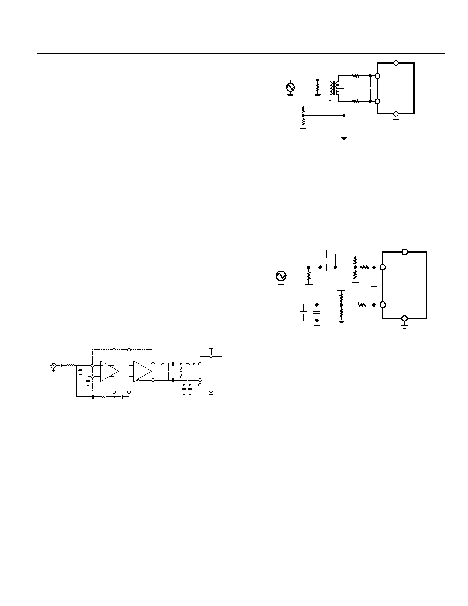
Optimum performance is achieved by driving the AD9229 in a
differential input configuration. For ultrasound applications,
the AD8332 differential driver provides excellent performance
and a flexible interface to the ADC (see Figure 37).
AD8332
1.0k
Ω
1.0k
Ω
374
Ω
187
Ω
04418-032
AD9229
VIN+
VIN–
AVDD
AGND
R
C
0.1
μF
187nH
VREF
0.1
μF
0.1
μF
0.1
μF
0.1
μF10μF
0.1
μF
1V p-p
0.1
μF
AVDD
LNA
120nH
VGA
VOH
VIP
INH
22p
LMD
VIN
LOP
LON
VOL
18nF
274
Ω
Figure 37. Differential Input Configuration Using the AD8332
However, the noise performance of most amplifiers is not
adequate to achieve the true performance of the AD9229. For
applications where SNR is a key parameter, differential transfor-
mer coupling is the recommended input configuration. An
example of this is shown in Figure 38.
In any configuration, the value of the shunt capacitor, C, is
dependent on the input frequency and may need to be reduced
or removed.
04418-033
AD9229
VIN+
VIN–
AVDD
AGND
2Vp-p
R
C
49.9
Ω
0.1
μF
1k
Ω
1k
Ω
AVDD
Figure 38. Differential Transformer—Coupled Configuration
Single-Ended Input Configuration
A single-ended input can provide adequate performance in
cost-sensitive applications. In this configuration, SFDR and
distortion performance degrade due to the large input
common-mode swing. However, if the source impedances
on each input are matched, there should be little effect on
SNR performance. Figure 39 details a typical single-ended
input configuration.
04418-
034
2V p-p
R
C
49.9
Ω
0.1
μF
10
μF
10
μF
0.1
μF
AD9229
VIN+
VIN–
AVDD
AGND
AVDD
1k
Ω
1k
Ω
1k
Ω
1k
Ω
Figure 39. Single-Ended Input Configuration
CLOCK INPUT CONSIDERATIONS
Typical high speed ADCs use both clock edges to generate a
variety of internal timing signals and, as a result, may be sensi-
tive to clock duty cycle. Typically, a 10% tolerance is required on
the clock duty cycle to maintain dynamic performance charac-
teristics. The AD9229 has a self-contained clock duty cycle
stabilizer that retimes the nonsampling edge, providing an
internal clock signal with a nominal 50% duty cycle. This allows
a wide range of clock input duty cycles without affecting the
performance of the AD9229.
An on-board phase-locked loop (PLL) multiplies the input
clock rate for the purpose of shifting the serial data out. The
stability criteria for the PLL limits the minimum sample clock
rate of the ADC to 10 MSPS. Assuming steady state operation of
the input clock, any sudden change in the sampling rate could
create an out-of-lock condition leading to invalid outputs at the
DCO, FCO, and data out pins.
相关PDF资料 |
PDF描述 |
|---|---|
| AD7870JP | IC ADC 12BIT SAMPLING 3V 28-PLCC |
| MS27467E21F35PB | CONN PLUG 79POS STRAIGHT W/PINS |
| D38999/20FA98PE | CONN RCPT 3POS WALL MNT W/PINS |
| AD7626BCPZ-RL7 | IC ADC 16BIT 10MSPS DIFF 32LFCSP |
| LTC2369IMS-18#TRPBF | IC ADC 18BIT SRL/SPI 16-MSOP |
相关代理商/技术参数 |
参数描述 |
|---|---|
| AD9229ABCPZRL7-65 | 功能描述:IC ADC 12BIT SRL 65MSPS 48LFCSP RoHS:是 类别:集成电路 (IC) >> 数据采集 - 模数转换器 系列:- 标准包装:1 系列:- 位数:14 采样率(每秒):83k 数据接口:串行,并联 转换器数目:1 功率耗散(最大):95mW 电压电源:双 ± 工作温度:0°C ~ 70°C 安装类型:通孔 封装/外壳:28-DIP(0.600",15.24mm) 供应商设备封装:28-PDIP 包装:管件 输入数目和类型:1 个单端,双极 |
| AD9229BBC-65 | 制造商:Analog Devices 功能描述:- Bulk |
| ad9229bcp-50 | 制造商:Analog Devices 功能描述: |
| AD9229BCP-65 | 制造商:Analog Devices 功能描述:- Bulk |
| AD9229BCPZ-50 | 制造商:Analog Devices 功能描述:ADC Quad Pipelined 50Msps 12-bit Serial 48-Pin LFCSP EP |
发布紧急采购,3分钟左右您将得到回复。