- 您现在的位置:买卖IC网 > PDF目录10073 > AD9229ABCPZRL7-50 (Analog Devices Inc)IC ADC 12BIT SRL 50MSPS 48LFCSP PDF资料下载
参数资料
| 型号: | AD9229ABCPZRL7-50 |
| 厂商: | Analog Devices Inc |
| 文件页数: | 13/40页 |
| 文件大小: | 0K |
| 描述: | IC ADC 12BIT SRL 50MSPS 48LFCSP |
| 标准包装: | 750 |
| 位数: | 12 |
| 采样率(每秒): | 50M |
| 数据接口: | 串行 |
| 转换器数目: | 4 |
| 功率耗散(最大): | 1.08W |
| 电压电源: | 模拟和数字 |
| 工作温度: | -40°C ~ 85°C |
| 安装类型: | 表面贴装 |
| 封装/外壳: | 48-VFQFN 裸露焊盘,CSP |
| 供应商设备封装: | 48-LFCSP-VQ(7x7) |
| 包装: | 带卷 (TR) |
| 输入数目和类型: | 8 个单端,单极;4 个差分,单极 |
第1页第2页第3页第4页第5页第6页第7页第8页第9页第10页第11页第12页当前第13页第14页第15页第16页第17页第18页第19页第20页第21页第22页第23页第24页第25页第26页第27页第28页第29页第30页第31页第32页第33页第34页第35页第36页第37页第38页第39页第40页
AD9229
Rev. B | Page 20 of 40
High speed, high resolution ADCs are sensitive to the quality of
the clock input. The degradation in SNR at a given full-scale
input frequency (fA) due only to aperture jitter (tA) can be
calculated with the following equation:
SNR degradation = 20 × log 10 [1/2 × π × fA × tA]
In the equation, the rms aperture jitter, tA, represents the root
sum square of all jitter sources, which include the clock input,
analog input signal, and ADC aperture jitter specification.
Applications that require undersampling are particularly
sensitive to jitter.
The clock input should be treated as an analog signal in cases
where aperture jitter may affect the dynamic range of the
AD9229. Power supplies for clock drivers should be separated
from the ADC output driver supplies to avoid modulating the
clock signal with digital noise. Low jitter, crystal-controlled
oscillators make the best clock sources. If the clock is generated
from another type of source (by gating, dividing, or other
methods), it should be retimed by the original clock at the
last step.
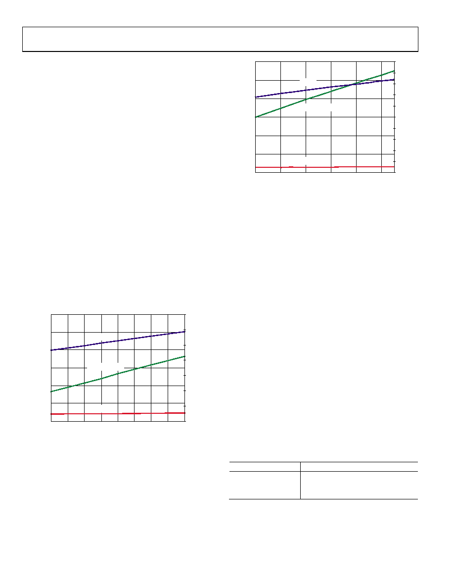
Power Dissipation and Power-Down Mode
the AD9229 is proportional to its sample rate. The digital power
dissipation does not vary much because it is determined
primarily by the DRVDD supply and bias current of the LVDS
output drivers.
ENCODE (MSPS)
P
O
WE
R
(mW)
1200
900
800
600
700
1000
1100
CURRE
NT
(mA)
350
250
0
100
50
200
150
300
10
50
40
45
30
35
20
25
15
04418-056
IAVDD
TOTAL POWER
IDRVDD
Figure 40. Supply Current vs. fSAMPLE for fIN = 10.3 MHz, fSAMPLE = 50 MSPS
ENCODE (MSPS)
POWER
(mW)
1400
1100
1000
800
900
1200
1300
CURRENT
(mA)
500
300
250
200
0
50
150
100
350
400
450
10
50
60
40
30
20
04418-
055
IAVDD
TOTAL POWER
IDRVDD
Figure 41. Supply Current vs. fSAMPLE for fIN = 10.3 MHz, fSAMPLE = 65 MSPS
By asserting the PDWN pin high, the AD9229 is placed in
power-down mode. In this state, the ADC typically dissipates
3 mW. During power-down, the LVDS output drivers are placed
in a high impedance state. Reasserting the PDWN pin low
returns the AD9229 to normal operating mode.
In power-down mode, low power dissipation is achieved by
shutting down the reference, reference buffer, PLL, and biasing
networks. The decoupling capacitors on REFT and REFB are
discharged when entering standby mode and then must be
recharged when returning to normal operation. As a result, the
wake-up time is related to the time spent in the power-down
mode; shorter cycles result in proportionally shorter wake-up
times. With the recommended 0.1 μF and 10 μF decoupling
capacitors on REFT and REFB, it takes approximately 1 sec to
fully discharge the reference buffer decoupling capacitors and
4 ms to restore full operation.
Digital Outputs
The AD9229’s differential outputs conform to the ANSI-644
LVDS standard. To set the LVDS bias current, place a resistor
(RSET is nominally equal to 4.0 kΩ) to ground at the
LVDSBIAS pin. The RSET resistor current is derived on-chip
and sets the output current at each output equal to a nominal
3.5 mA. A 100 Ω differential termination resistor placed at the
LVDS receiver inputs results in a nominal 350 mV swing at the
receiver. To adjust the differential signal swing, simply change
the resistor to a different value, as shown in Table 7.
Table 7. LVDSBIAS Pin Configuration
RSET
Differential Output Swing
3.7 kΩ
375 mV p-p
4.0 kΩ (default)
350 mV p-p
4.3 kΩ
325 mV p-p
相关PDF资料 |
PDF描述 |
|---|---|
| AD7870JP | IC ADC 12BIT SAMPLING 3V 28-PLCC |
| MS27467E21F35PB | CONN PLUG 79POS STRAIGHT W/PINS |
| D38999/20FA98PE | CONN RCPT 3POS WALL MNT W/PINS |
| AD7626BCPZ-RL7 | IC ADC 16BIT 10MSPS DIFF 32LFCSP |
| LTC2369IMS-18#TRPBF | IC ADC 18BIT SRL/SPI 16-MSOP |
相关代理商/技术参数 |
参数描述 |
|---|---|
| AD9229ABCPZRL7-65 | 功能描述:IC ADC 12BIT SRL 65MSPS 48LFCSP RoHS:是 类别:集成电路 (IC) >> 数据采集 - 模数转换器 系列:- 标准包装:1 系列:- 位数:14 采样率(每秒):83k 数据接口:串行,并联 转换器数目:1 功率耗散(最大):95mW 电压电源:双 ± 工作温度:0°C ~ 70°C 安装类型:通孔 封装/外壳:28-DIP(0.600",15.24mm) 供应商设备封装:28-PDIP 包装:管件 输入数目和类型:1 个单端,双极 |
| AD9229BBC-65 | 制造商:Analog Devices 功能描述:- Bulk |
| ad9229bcp-50 | 制造商:Analog Devices 功能描述: |
| AD9229BCP-65 | 制造商:Analog Devices 功能描述:- Bulk |
| AD9229BCPZ-50 | 制造商:Analog Devices 功能描述:ADC Quad Pipelined 50Msps 12-bit Serial 48-Pin LFCSP EP |
发布紧急采购,3分钟左右您将得到回复。