- 您现在的位置:买卖IC网 > PDF目录1986 > AD9248BCPZRL-65 (Analog Devices Inc)IC ADC 14BIT DUAL 65MSPS 64LFCSP PDF资料下载
参数资料
| 型号: | AD9248BCPZRL-65 |
| 厂商: | Analog Devices Inc |
| 文件页数: | 13/48页 |
| 文件大小: | 0K |
| 描述: | IC ADC 14BIT DUAL 65MSPS 64LFCSP |
| 标准包装: | 2,500 |
| 位数: | 14 |
| 采样率(每秒): | 65M |
| 数据接口: | 并联 |
| 转换器数目: | 2 |
| 功率耗散(最大): | 600mW |
| 电压电源: | 单电源 |
| 工作温度: | -40°C ~ 85°C |
| 安装类型: | 表面贴装 |
| 封装/外壳: | 64-VFQFN 裸露焊盘,CSP |
| 供应商设备封装: | 64-LFCSP-VQ(9x9) |
| 包装: | 带卷 (TR) |
| 输入数目和类型: | 4 个单端,单极;2 个差分,单极 |
第1页第2页第3页第4页第5页第6页第7页第8页第9页第10页第11页第12页当前第13页第14页第15页第16页第17页第18页第19页第20页第21页第22页第23页第24页第25页第26页第27页第28页第29页第30页第31页第32页第33页第34页第35页第36页第37页第38页第39页第40页第41页第42页第43页第44页第45页第46页第47页第48页
AD9248
Rev. B | Page 20 of 48
DATA FORMAT
The AD9248 data output format can be configured for either
twos complement or offset binary. This is controlled by the data
format select pin (DFS). Connecting DFS to AGND produces
offset binary output data. Conversely, connecting DFS to AVDD
formats the output data as twos complement.
The output data from the dual ADCs can be multiplexed onto a
single 14-bit output bus. The multiplexing is accomplished by
toggling the MUX_SELECT bit, which directs channel data to
the same or opposite channel data port. When MUX_SELECT
is logic high, the Channel A data is directed to the Channel A
output bus, and the Channel B data is directed to the Channel B
output bus. When MUX_SELECT is logic low, the channel data
is reversed, that is, the Channel A data is directed to the
Channel B output bus, and the Channel B data is directed to the
Channel A output bus. By toggling the MUX_SELECT bit,
multiplexed data is available on either of the output data ports.
If the ADCs run with synchronized timing, this same clock can
be applied to the MUX_SELECT pin. Any skew between
CLK_A, CLK_B, and MUX_SELECT can degrade AC
performance. It is recommended to keep the clock skew
<100 pS. After the MUX_SELECT rising edge, either data port
has the data for its respective channel; after the falling edge, the
alternate channel’s data is placed on the bus. Typically, the other
unused bus would be disabled by setting the appropriate OEB
high to reduce power consumption and noise. Figure 34 shows
an example of multiplex mode. When multiplexing data, the
data rate is two times the sample rate. Note that both channels
must remain active in this mode and that each channel’s power-
down pin must remain low.
VOLTAGE REFERENCE
A stable and accurate 0.5 V voltage reference is built into the
AD9248. The input range can be adjusted by varying the
reference voltage applied to the AD9248, using either the
internal reference with different external resistor configurations
or an externally applied reference voltage. The input span of the
ADC tracks reference voltage changes linearly. If the ADC is
being driven differentially through a transformer, the reference
voltage can be used to bias the center tap (common-mode
voltage).
The shared reference mode allows the user to connect the
references from the dual ADCs together externally for superior
gain and offset matching performance. If the ADCs are to
function independently, the reference decoupling can be
treated independently and can provide superior isolation
between the dual channels. To enable shared reference mode,
the SHARED_REF pin must be tied high and the external
differential references must be externally shorted. (REFT_A
must be externally shorted to REFT_B, and REFB_A must be
shorted to REFB_B.)
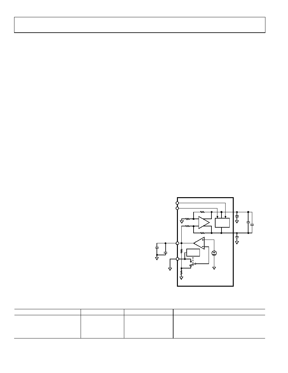
Internal Reference Connection
A comparator within the AD9248 detects the potential at the
SENSE pin and configures the reference into four possible
states, which are summarized in Table 7. If SENSE is grounded,
the reference amplifier switch is connected to the internal
resistor divider (see Figure 35), setting VREF to 1 V.
Connecting the SENSE pin to VREF switches the reference
amplifier output to the SENSE pin, completing the loop and
providing a 0.5 V reference output. If a resistor divider is
connected, as shown in Figure 36, the switch is again set to the
SENSE pin. This puts the reference amplifier in a noninverting
mode with the VREF output defined as
VREF = 0.5 × (1 + R2/R1)
In all reference configurations, REFT and REFB drive the ADC
core and establish its input span. The input range of the ADC
always equals twice the voltage at the reference pin for either an
internal or an external reference.
VIN+
VIN–
10
μF
10
μF
0.1
μF
0.1
μF
REFT
ADC
CORE
SELECT
LOGIC
SENSE
0.1
μF
0.5V
AD9248
REFB
0.1
μF
VREF
04446-
034
Figure 35. Internal Reference Configuration
Table 7. Reference Configuration Summary
Selected Mode
SENSE Voltage
Resulting VREF (V)
Resulting Differential Span (V p-p)
External Reference
AVDD
N/A
2 × External Reference
Internal Fixed Reference
VREF
0.5
1.0
Programmable Reference
0.2 V to VREF
0.5 × (1 + R2/R1)
Internal Fixed Reference
AGND to 0.2 V
1.0
2.0
相关PDF资料 |
PDF描述 |
|---|---|
| AD9251BCPZ-65 | IC ADC 14BIT 65MSPS 64LFCSP |
| AD9252ABCPZRL7-50 | IC ADC 14BIT SRL 50MSPS 64LFCSP |
| AD9253TCPZ-125EP | IC ADC 14BIT SRL 125MSPS 48LFCSP |
| AD9257BCPZ-65 | IC ADC 14BIT SRL 65MSPS 64LFCSP |
| AD9258BCPZ-125 | IC ADC 14BIT 125MSPS DL 64LFCSP |
相关代理商/技术参数 |
参数描述 |
|---|---|
| AD9248BCPZRL7-20 | 制造商:AD 制造商全称:Analog Devices 功能描述:14-Bit, 20/40/65 MSPS Dual A/ D Converter |
| AD9248BCPZRL7-40 | 制造商:AD 制造商全称:Analog Devices 功能描述:14-Bit, 20/40/65 MSPS Dual A/ D Converter |
| AD9248BCPZRL7-65 | 制造商:AD 制造商全称:Analog Devices 功能描述:14-Bit, 20/40/65 MSPS Dual A/ D Converter |
| AD9248BST-20 | 制造商:AD 制造商全称:Analog Devices 功能描述:14-Bit, 20/40/65 MSPS Dual A/ D Converter |
| AD9248BST-40 | 制造商:AD 制造商全称:Analog Devices 功能描述:14-Bit, 20/40/65 MSPS Dual A/ D Converter |
发布紧急采购,3分钟左右您将得到回复。