- 您现在的位置:买卖IC网 > PDF目录1986 > AD9252ABCPZRL7-50 (Analog Devices Inc)IC ADC 14BIT SRL 50MSPS 64LFCSP PDF资料下载
参数资料
| 型号: | AD9252ABCPZRL7-50 |
| 厂商: | Analog Devices Inc |
| 文件页数: | 1/52页 |
| 文件大小: | 0K |
| 描述: | IC ADC 14BIT SRL 50MSPS 64LFCSP |
| 标准包装: | 750 |
| 位数: | 14 |
| 采样率(每秒): | 50M |
| 数据接口: | 串行,SPI? |
| 转换器数目: | 8 |
| 功率耗散(最大): | 773mW |
| 电压电源: | 模拟和数字 |
| 工作温度: | -40°C ~ 85°C |
| 安装类型: | 表面贴装 |
| 封装/外壳: | 64-VFQFN 裸露焊盘,CSP |
| 供应商设备封装: | 64-LFCSP-VQ(9x9) |
| 包装: | 带卷 (TR) |
| 输入数目和类型: | 16 个单端,单极;8 个差分,单极 |
当前第1页第2页第3页第4页第5页第6页第7页第8页第9页第10页第11页第12页第13页第14页第15页第16页第17页第18页第19页第20页第21页第22页第23页第24页第25页第26页第27页第28页第29页第30页第31页第32页第33页第34页第35页第36页第37页第38页第39页第40页第41页第42页第43页第44页第45页第46页第47页第48页第49页第50页第51页第52页
Octal, 14-Bit, 50 MSPS,
Serial LVDS, 1.8 V ADC
Data Sheet
Rev. E
Information furnished by Analog Devices is believed to be accurate and reliable. However, no
responsibilityis assumedbyAnalogDevicesforitsuse,norforanyinfringementsof patentsorother
rightsofthirdpartiesthatmayresultfromitsuse.Specificationssubjecttochangewithoutnotice.No
license is granted by implication or otherwise under any patent or patent rights of Analog Devices.
Trademarksandregisteredtrademarksarethepropertyoftheirrespectiveowners.
One Technology Way, P.O. Box 9106, Norwood, MA 02062-9106, U.S.A.
Tel: 781.329.4700
Fax: 781.461.3113
2006–2011 Analog Devices, Inc. All rights reserved.
FEATURES
8 analog-to-digital converters (ADCs) integrated into 1 package
93.5 mW ADC power per channel at 50 MSPS
SNR = 73 dB (to Nyquist)
ENOB = 12 bits
SFDR = 84 dBc (to Nyquist)
Excellent linearity
DNL = ±0.4 LSB (typical); INL = ±1.5 LSB (typical)
Serial LVDS (ANSI-644, default)
Low power, reduced signal option (similar to IEEE 1596.3)
Data and frame clock outputs
325 MHz, full-power analog bandwidth
2 V p-p input voltage range
1.8 V supply operation
Serial port control
Full-chip and individual-channel power-down modes
Flexible bit orientation
Built-in and custom digital test pattern generation
Programmable clock and data alignment
Programmable output resolution
Standby mode
APPLICATIONS
Medical imaging and nondestructive ultrasound
Portable ultrasound and digital beam-forming systems
Quadrature radio receivers
Diversity radio receivers
Tape drives
Optical networking
Test equipment
GENERAL DESCRIPTION
The AD9252 is an octal, 14-bit, 50 MSPS ADC with an on-chip
sample-and-hold circuit designed for low cost, low power, small size,
and ease of use. Operating at a conversion rate of up to 50 MSPS,
it is optimized for outstanding dynamic performance and low
power in applications where a small package size is critical.
The ADC requires a single 1.8 V power supply and LVPECL-/
CMOS-/LVDS-compatible sample rate clock for full performance
operation. No external reference or driver components are
required for many applications.
The ADC automatically multiplies the sample rate clock for
the appropriate LVDS serial data rate. A data clock (DCO)
for capturing data on the output and a frame clock (FCO) for
signaling a new output byte are provided. Individual channel
power-down is supported and typically consumes less than
2 mW when all channels are disabled.
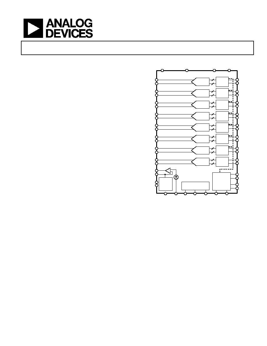
FUNCTIONAL BLOCK DIAGRAM
SERIAL
LVDS
REF
SELECT
AD9252
AGND
VIN – A
VIN + A
VIN – B
VIN + B
VIN – D
VIN + D
VIN – C
VIN + C
SENSE
VREF
AVDD
DRVDD
14
PDWN
REFT
REFB
D – A
D + A
D – B
D + B
D – D
D + D
D – C
D + C
FCO–
FCO+
DCO+
DCO–
CLK+
DRGND
CLK–
SERIAL PORT
INTERFACE
CSB
SCLK/
DTP
SDIO/
ODM
RBIAS
SERIAL
LVDS
SERIAL
LVDS
SERIAL
LVDS
ADC
DATA RATE
MULTIPLIER
0.5V
SERIAL
LVDS
VIN – E
VIN + E
VIN – F
VIN + F
VIN – H
VIN + H
VIN – G
VIN + G
14
D – E
D + E
D – F
D + F
D – H
D + H
D – G
D + G
SERIAL
LVDS
SERIAL
LVDS
SERIAL
LVDS
ADC
062
96-
001
Figure 1.
The ADC contains several features designed to maximize
flexibility and minimize system cost, such as programmable
clock and data alignment and programmable digital test pattern
generation. The available digital test patterns include built-in
deterministic and pseudorandom patterns, along with custom user-
defined test patterns entered via the serial port interface (SPI).
The AD9252 is available in an RoHS compliant, 64-lead LFCSP. It is
specified over the industrial temperature range of 40°C to +85°C.
PRODUCT HIGHLIGHTS
1.
Small Footprint. Eight ADCs are contained in a small package.
2.
Low Power of 93.5 mW per Channel at 50 MSPS.
3.
Ease of Use. A data clock output (DCO) operates up to
350 MHz and supports double data rate (DDR) operation.
4.
User Flexibility. SPI control offers a wide range of flexible
features to meet specific system requirements.
5.
Pin-Compatible Family. This includes the AD9212 (10-bit)
and AD9222 (12-bit).
相关PDF资料 |
PDF描述 |
|---|---|
| AD9253TCPZ-125EP | IC ADC 14BIT SRL 125MSPS 48LFCSP |
| AD9257BCPZ-65 | IC ADC 14BIT SRL 65MSPS 64LFCSP |
| AD9258BCPZ-125 | IC ADC 14BIT 125MSPS DL 64LFCSP |
| AD9259ABCPZRL7-50 | IC ADC 14BIT SRL 50MSPS 48LFCSP |
| AD9260ASZRL | IC ADC 16BIT 2.5MHZ 44MQFP |
相关代理商/技术参数 |
参数描述 |
|---|---|
| AD9252BCPZ-50 | 制造商:Analog Devices 功能描述:IC ((NW)) 制造商:Analog Devices 功能描述:IC,A/D CONVERTER,OCTAL,14-BIT,LLCC,64PIN |
| AD9252BCPZRL7-50 | 制造商:AD 制造商全称:Analog Devices 功能描述:Octal, 14-Bit, 50 MSPS Serial LVDS 1.8 V A/D Converter |
| AD9253 | 制造商:AD 制造商全称:Analog Devices 功能描述:Quad, 14-Bit, 80 MSPS/105 MSPS/125 MSPS |
| AD9253-125EBZ | 功能描述:BOARD EVAL FOR AD9253-125 RoHS:是 类别:编程器,开发系统 >> 评估板 - 模数转换器 (ADC) 系列:- 产品培训模块:Obsolescence Mitigation Program 标准包装:1 系列:- ADC 的数量:1 位数:12 采样率(每秒):94.4k 数据接口:USB 输入范围:±VREF/2 在以下条件下的电源(标准):- 工作温度:-40°C ~ 85°C 已用 IC / 零件:MAX11645 已供物品:板,软件 |
| AD9253BCPZ-105 | 功能描述:IC ADC 14BIT SRL 105MSPS 48LFCSP RoHS:是 类别:集成电路 (IC) >> 数据采集 - 模数转换器 系列:- 其它有关文件:TSA1204 View All Specifications 标准包装:1 系列:- 位数:12 采样率(每秒):20M 数据接口:并联 转换器数目:2 功率耗散(最大):155mW 电压电源:模拟和数字 工作温度:-40°C ~ 85°C 安装类型:表面贴装 封装/外壳:48-TQFP 供应商设备封装:48-TQFP(7x7) 包装:Digi-Reel® 输入数目和类型:4 个单端,单极;2 个差分,单极 产品目录页面:1156 (CN2011-ZH PDF) 其它名称:497-5435-6 |
发布紧急采购,3分钟左右您将得到回复。