参数资料
| 型号: | AD9267BCPZ |
| 厂商: | Analog Devices Inc |
| 文件页数: | 23/24页 |
| 文件大小: | 0K |
| 描述: | IC MOD SIGMA-DELTA DUAL 64LFCSP |
| 标准包装: | 1 |
| 类型: | 三角积分调制器 |
| 应用: | 无线通信系统 |
| 安装类型: | 表面贴装 |
| 封装/外壳: | 64-VFQFN 裸露焊盘,CSP |
| 供应商设备封装: | 64-LFCSP-VQ(9x9) |
| 包装: | 托盘 |
AD9267
Rev. 0 | Page 8 of 24
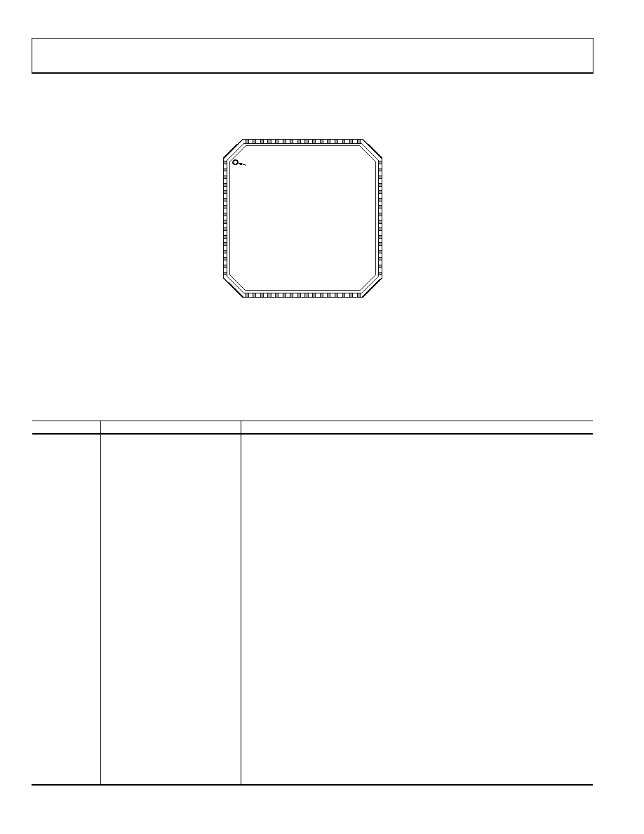
PIN CONFIGURATION AND FUNCTION DESCRIPTIONS
NOTES
1. DNC = DO NOT CONNECT.
2. THE EXPOSED PAD MUST BE SOLDERED TO THE GROUND PLANE FOR THE
LFCSP PACKAGE. SOLDERING THE EXPOSED PADDLE TO THE PCB
INCREASES THE RELIABILITY OF THE SOLDER JOINTS, MAXIMIZING
THE THERMAL CAPACITY OF THE PACKAGE.
PIN 1
INDICATOR
17
18
19
20
21
22
23
24
25
26
27
28
29
30
31
32
OR
–
B
OR
+
B
DCO
–
DCO
+
DNC
DR
VD
D
DG
ND
DV
DD
DNC
OR
–
A
OR
+
A
64
63
62
61
60
59
58
57
56
55
54
53
52
51
50
49
CL
K
+
CG
ND
AG
ND
AV
D
VI
N
–
B
VI
N
+
B
AV
D
CF
IL
T
VR
E
F
AV
D
VI
N
–
A
VI
N
+
A
AV
D
AG
ND
RE
S
E
T
CS
B
1
2
3
4
5
6
7
8
9
10
11
12
13
14
15
16
CLK–
CVDD
PDWNA
PDWNB
PLL_LOCKED
DVDD
DGND
DRVDD
D0–B
D0+B
D1–B
D1+B
D2–B
D2+B
D3–B
D3+B
SCLK/PLLMULT0
SDIO/PLLMULT1
PLLMULT2
PLLMULT3
PLLMULT4
DVDD
DGND
DRVDD
D3+A
D3–A
D2+A
D2–A
D1+A
D1–A
D0+A
D0–A
48
47
46
45
44
43
42
41
40
39
38
37
36
35
34
33
AD9267
TOP VIEW
(Not to Scale)
0
77
73
-00
3
Figure 3. Pin Configuration
Table 7. Pin Function Descriptions
Pin No.
Mnemonic
Description
1
CLK
Differential Clock Input ().
2
CVDD
Clock Supply (1.8 V).
3, 4
PDWNA, PDWNB
Power-Down Pins. Active high.
5
PLL_LOCKED
PLL Lock Indicator.
6, 25, 43
DVDD
Digital Supply (1.8 V).
7, 24, 42
DGND
Digital Ground.
8, 23, 41
DRVDD
Digital Output Driver Supply
9 to 16
D0B, D0+B to D3B, D3+B
Channel B Differential LVDS Data Output Bits. D0+B is the LSB and D3+B is the MSB.
17, 18
ORB, OR+B
Channel B Overrange Indicator Pins.
19, 20
DCO, DCO+
Differential Data Clock Output.
21, 22, 26 to 30
DNC
Do Not Connect.
31, 32
ORA, OR+A
Channel A Overrange Indicator Pins.
33 to 40
D0A, D0+A to D3A, D3+A
Channel A Differential LVDS Data Output Bits. D0+A is the LSB and D3+A is the MSB.
44, 45, 46
PLLMULT4, PLLMULT3, PLLMULT2
PLL Mode Selection Pins.
47
SDIO/PLLMULT1
Serial Port Interface Data Input/Output/PLL Mode Selection Pins.
48
SCLK/PLLMULT0
Serial Port Interface Clock/PLL Mode Selection Pins.
49
CSB
Serial Port Interface Chip Select Pin Active Low.
50
RESET
Chip Reset.
51, 62
AGND
Analog Ground.
52, 55, 58, 61
AVDD
Analog Supply (1.8 V).
53, 54
VIN+A, VINA
Channel A Analog Input.
56
VREF
Voltage Reference Input.
57
CFILT
Noise Limiting Filter Capacitor.
59, 60
VIN+B, VINB
Channel B Analog Input.
63
CGND
Clock Ground.
64
CLK+
Differential Clock Input (+).
65
Exposed paddle (EPAD)
Analog Ground. (Pin 65 is the exposed thermal pad on the bottom of the package.) The
exposed paddle must be soldered to analog ground of the PCB to achieve optimal electrical
and thermal performance.
相关PDF资料 |
PDF描述 |
|---|---|
| AD9272BSVZRL-80 | IC ADC ASD OCTAL 80MSPS 100-TQFP |
| AD9273BBCZ-50 | IC ADCASD OCTAL 25MSPS 144CSPBGA |
| AD9276BSVZ | IC ADC 12BIT LNA/VGA/AAF 100TQFP |
| AD9277BSVZ | IC ADC 14BIT LNA/VGA/AAF 100TQFP |
| AD9278BBCZ | IC ADC 12BIT 50MSPS 144CSPBGA |
相关代理商/技术参数 |
参数描述 |
|---|---|
| AD9267BCPZRL7 | 功能描述:IC MOD SIGMA-DELTA DUAL 64LFCSP RoHS:是 类别:集成电路 (IC) >> 专用 IC 系列:- 产品培训模块:Lead (SnPb) Finish for COTS Obsolescence Mitigation Program 标准包装:1 系列:- 类型:调帧器 应用:数据传输 安装类型:表面贴装 封装/外壳:400-BBGA 供应商设备封装:400-PBGA(27x27) 包装:散装 |
| AD9267EBZ | 功能描述:BOARD EVALUATION FOR AD9267 RoHS:是 类别:编程器,开发系统 >> 评估板 - 模数转换器 (ADC) 系列:- 产品培训模块:Obsolescence Mitigation Program 标准包装:1 系列:- ADC 的数量:1 位数:12 采样率(每秒):94.4k 数据接口:USB 输入范围:±VREF/2 在以下条件下的电源(标准):- 工作温度:-40°C ~ 85°C 已用 IC / 零件:MAX11645 已供物品:板,软件 |
| AD9268 | 制造商:AD 制造商全称:Analog Devices 功能描述:16-Bit, 80 MSPS/105 MSPS/125 MSPS, 1.8 V Dual Analog-to-Digital Converter (ADC) |
| AD9268-105EBZ1 | 制造商:AD 制造商全称:Analog Devices 功能描述:16-Bit, 80 MSPS/105 MSPS/125 MSPS, 1.8 V Dual Analog-to-Digital Converter (ADC) |
| AD9268-125EBZ | 功能描述:数据转换 IC 开发工具 Dual 16 bit 125 high SNR ADC RoHS:否 制造商:Texas Instruments 产品:Demonstration Kits 类型:ADC 工具用于评估:ADS130E08 接口类型:SPI 工作电源电压:- 6 V to + 6 V |
发布紧急采购,3分钟左右您将得到回复。