- 您现在的位置:买卖IC网 > PDF目录10689 > AD9280ARSZ (Analog Devices Inc)IC ADC CMOS 8BIT 32MSPS 28-SSOP PDF资料下载
参数资料
| 型号: | AD9280ARSZ |
| 厂商: | Analog Devices Inc |
| 文件页数: | 5/24页 |
| 文件大小: | 0K |
| 描述: | IC ADC CMOS 8BIT 32MSPS 28-SSOP |
| 产品变化通告: | AD9280 Pin Configuration Description Change 21/Apr/2010 |
| 标准包装: | 47 |
| 位数: | 8 |
| 采样率(每秒): | 32M |
| 数据接口: | 并联 |
| 转换器数目: | 1 |
| 功率耗散(最大): | 110mW |
| 电压电源: | 单电源 |
| 工作温度: | -40°C ~ 85°C |
| 安装类型: | 表面贴装 |
| 封装/外壳: | 28-SSOP(0.209",5.30mm 宽) |
| 供应商设备封装: | 28-SSOP |
| 包装: | 管件 |
| 输入数目和类型: | 1 个单端,单极 |
| 产品目录页面: | 780 (CN2011-ZH PDF) |
AD9280
–13–
The allowable voltage range that can be applied to CLAMPIN
depends on the operational limits of the internal clamp ampli-
fier. The recommended clamp range is between 0.5 volts and
2.0 volts.
The input capacitor should be sized to allow sufficient acquisi-
tion time of the clamp voltage at AIN within the CLAMP inter-
val, but also be sized to minimize droop between clamping
intervals. Specifically, the acquisition time when the switch is
closed will equal:
T ACQ = RINCIN ln
VC
VE
where VC is the voltage change required across CIN, and VE is
the error voltage. VC is calculated by taking the difference be-
tween the initial input dc level at the start of the clamp interval
and the clamp voltage supplied at CLAMPIN. VE is a system
dependent parameter, and equals the maximum tolerable devia-
tion from VC. For example, if a 2-volt input level needs to be
clamped to 1 volt at the AD9280’s input within 10 millivolts,
then VC equals 2 – 1 or 1 volt, and VE equals 10 mV. Note that
once the proper clamp level is attained at the input, only a very
small voltage change will be required to correct for droop.
The voltage droop is calculated with the following equation:
dV
=
IBIAS
CIN
t
()
where t = time between clamping intervals.
The bias current of the AD9280 will depend on the sampling
rate, FS, and the difference between the reference midpoint,
(REFTS–REFBS)/2 and the input voltage. For a fixed sampling
rate of 32 MHz, Figure 14 shows the input bias current for a
given input. For a 1 V input range, the maximum input bias
current from Figure 14 is 22
A. For lower sampling rates the
input bias current will scale proportionally.
If droop is a critical parameter, then the minimum value of CIN
should be calculated first based on the droop requirement.
Acquisition time—the width of the CLAMP pulse—can be
adjusted accordingly once the minimum capacitor value is cho-
sen. A tradeoff will often need to be made between droop and
acquisition time, or error voltage VE.
Clamp Circuit Example
A single supply video amplifier outputs a level-shifted video
signal between 2 and 3 volts with the following parameters:
horizontal period = 63.56
s,
horizontal sync interval = 10.9
s,
horizontal sync pulse = 4.7
s,
sync amplitude = 0.3 volts,
video amplitude of 0.7 volts,
reference black level = 2.3 volts
The video signal must be dc restored from a 2- to 3-volt range
down to a 1- to 2-volt range. Configuring the AD9280 for a
one volt input span with an input range from 1 to 2 volts (see
Figure 24), the CLAMPIN voltage can be set to 1 volt with an
external voltage or by direct connection to REFBS. The CLAMP
pulse may be applied during the SYNC pulse, or during the
back porch to truncate the SYNC below the AD9280’s mini-
mum input voltage. With a CIN = 1 F, and RIN = 20 , the
acquisition time needed to set the input dc level to one volt
with 1 mV accuracy is about 140
s, assuming a full 1 volt V
C.
With a 1
F input coupling capacitor, the droop across one
horizontal can be calculated:
IBIAS = 22 A, and t = 63.5 s, so dV = 1.397 mV, which is less
than one LSB.
After the input capacitor is initially charged, the clamp pulse
width only needs to be wide enough to correct small voltage
errors such as the droop. The fine scale settling characteristics
of the clamp circuitry are shown in Table II.
Depending on the required accuracy, a CLAMP pulse width of
1
s–3 s should work in most applications. The OFFSET val-
ues ignore the contribution of offset from the clamp amplifier;
they simply compare the output code with a “final value” mea-
sured with a much longer CLAMP pulse duration.
Table II.
CLAMP
OFFSET
8
s
<1 LSB
4
s
<2 LSBs
3
s
2 LSBs
2
s
5 LSBs
1
s
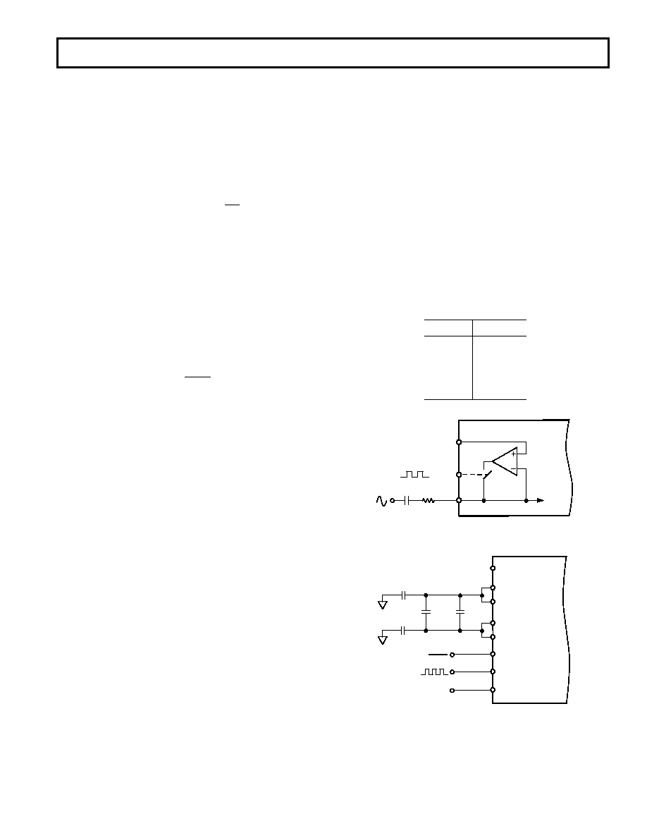
9 LSBs
CLAMP IN
AD9280
CLAMP
AIN
CIN
RIN
TO
SHA
SW1
Figure 24a. Clamp Operation
0.1 F
10 F
AIN
REFTF
REFBS
MODE
AD9280
REFTS
0.1 F
REFBF
CLAMP
CLAMPIN
AVDD
2
SHORT TO REFBS
OR EXTERNAL DC
0.1 F
Figure 24b. Video Clamp Circuit
REV. E
相关PDF资料 |
PDF描述 |
|---|---|
| ICL3222ECAZ | TRANSMITTER/RCVR RS232 LP 20SSOP |
| LTC1440CMS8 | IC COMP W/REF LP SINGLE 8-MSOP |
| AD7266BCPZ-REEL7 | IC ADC 12BIT 2MSPS 3CH 32LFCSP |
| ICL3222CAZ | TRANSMITTER/RCVR RS232 LP 20SSOP |
| ICL3222EIBZ | IC 2DRVR/2RCVR RS232 3V 18-SOIC |
相关代理商/技术参数 |
参数描述 |
|---|---|
| AD9280ARSZRL | 功能描述:IC ADC 8BIT CMOS 32MSPS 28SSOP RoHS:是 类别:集成电路 (IC) >> 数据采集 - 模数转换器 系列:- 标准包装:2,500 系列:- 位数:16 采样率(每秒):15 数据接口:MICROWIRE?,串行,SPI? 转换器数目:1 功率耗散(最大):480µW 电压电源:单电源 工作温度:-40°C ~ 85°C 安装类型:表面贴装 封装/外壳:38-WFQFN 裸露焊盘 供应商设备封装:38-QFN(5x7) 包装:带卷 (TR) 输入数目和类型:16 个单端,双极;8 个差分,双极 配用:DC1011A-C-ND - BOARD DELTA SIGMA ADC LTC2494 |
| AD9280-EB | 制造商:Analog Devices 功能描述:EVAL BD FOR AD9280 - Bulk |
| AD9280JRS | 制造商:未知厂家 制造商全称:未知厂家 功能描述:Analog-to-Digital Converter, 8-Bit |
| AD9280JRSRL | 制造商:未知厂家 制造商全称:未知厂家 功能描述:Analog-to-Digital Converter, 8-Bit |
| AD9281 | 制造商:AD 制造商全称:Analog Devices 功能描述:Dual Channel 8-Bit Resolution CMOS ADC |
发布紧急采购,3分钟左右您将得到回复。