- 您现在的位置:买卖IC网 > PDF目录10528 > AD9480ASUZ-250 (Analog Devices Inc)IC ADC 8BIT 250MSPS 3.3V 44TQFP PDF资料下载
参数资料
| 型号: | AD9480ASUZ-250 |
| 厂商: | Analog Devices Inc |
| 文件页数: | 11/28页 |
| 文件大小: | 0K |
| 描述: | IC ADC 8BIT 250MSPS 3.3V 44TQFP |
| 标准包装: | 1 |
| 位数: | 8 |
| 采样率(每秒): | 250M |
| 数据接口: | 并联 |
| 转换器数目: | 1 |
| 功率耗散(最大): | 590mW |
| 电压电源: | 单电源 |
| 工作温度: | -40°C ~ 85°C |
| 安装类型: | 表面贴装 |
| 封装/外壳: | 44-TQFP |
| 供应商设备封装: | 44-TQFP(10x10) |
| 包装: | 托盘 |
| 输入数目和类型: | 2 个单端,单极;2 个差分,单极 |
第1页第2页第3页第4页第5页第6页第7页第8页第9页第10页当前第11页第12页第13页第14页第15页第16页第17页第18页第19页第20页第21页第22页第23页第24页第25页第26页第27页第28页
AD9480
Rev. A | Page 19 of 28
AD9480 EVALUATION BOARD
The AD9480 evaluation board offers an easy way to test the
device. It requires a clock source, an analog input signal, and a
3.3 V power supply. The clock source is buffered on the board
to provide the clocks for the ADC and a data-ready signal. The
digital outputs and output clocks are available at a 40-pin
connector, P10. The board has several modes of operation and
is shipped in the following configuration:
Offset binary
Internal voltage reference
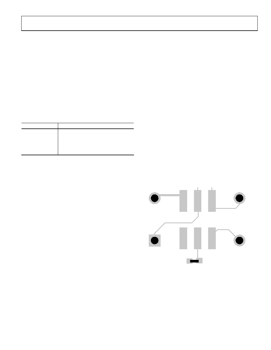
POWER CONNECTOR
Power is supplied to the board via two detachable 4-pin
power strips.
Table 11. Power Connector
Terminal
Comments
Analog supply for ADC ~ 150 mA
Output supply for ADC ~ 40 mA
VCTRL1, 2 3.3 V
Supply for support clock circuitry ~ 50 mA
Op Amp,
External Reference
Optional supply for op amp and
ADR510 reference
1 AVDD, DRVDD, and VCTRL are the minimum required power connections.
2 LVEL16 clock buffer can be powered from AVDD or VCTRL LVEL16 buffer
jumper.
ANALOG INPUTS
The evaluation board accepts a 700 mV p-p analog input signal
centered at ground at SMB Connector J3. This signal is
terminated to ground through 50 by R22. The input can be
alternatively terminated at the T1 transformer secondary by
R21 and R28. T1 is a wideband RF transformer that provides
the single-ended-to-differential conversion, allows the ADC to
be driven differentially, and minimizes even-order harmonics.
An optional transformer, T4, can be placed, if desired (remove
T1, as shown in Figure 41 and Figure 42).
The analog signal can be low-pass filtered by R31, C8, and
R29, C9 at the ADC input.
GAIN
Full scale is set by the sense jumper. This jumper applies a bias
to the SENSE pin to vary the full-scale range; the default
position is SENSE = ground, setting the full scale to 1 V p-p.
OPTIONAL OPERATIONAL AMPLIFIER
The PCB has been designed to accommodate an optional
AD8351 op amp, which can serve as a convenient solution for
dc-coupled applications. To use the AD8351 op amp, remove
R29, R31, and C3. Populate R40, R43, and R47 with 25
resistors, and populate C24, C28, C29, C30, C31, and C32 with
0.1 F capacitors. Populate R38, R39, and R51 with a 10
resistor, and R44 and R45 with a 1 k resistor. Populate R41
with a 1.2 k resistor and R42 with a 100 resistor. Populate
R52 with a 10 k resistor.
CLOCK
The clock input is terminated to ground through 50 at SMA
Connector J1. The input is ac-coupled to a high speed
differential receiver (LVEL16) that provides the required low
jitter and fast edge rates needed for best performance. J1 input
should be >0.5 V p-p. Power to the LVEL16 is set to VCTRL
(default) or AVDD by jumper placement at the device.
OPTIONAL CLOCK BUFFER
The PCB has been designed to accommodate the SNLVDS1
line driver. The SNLVDS1 is used as a high speed LVDS-level
optional encode clock. To use this clock, remove C2, C5, and
C6. Place a 0.1 F capacitor on C34, C35, and C26. Place a 10
resistor on R48, a 100 resistor on R6, and a 0 resistor on
R49 and R53. For best results using the LVDS line driver, J1
input should be >2.5 V p-p.
OPTIONAL XTAL
The PCB has been designed to accommodate an optional
crystal oscillator that can serve as a convenient clock source.
The footprint can accept both through-hole and surface-mount
devices, including Vectron XO-400 and Vectron VCC6 family
oscillators.
04619-040
VCC
OUT–
OUT+
GND
Figure 40. XTAL Footprint
To use either crystal, populate C26 and C27 with 0.1 F capaci-
tors. Populate R49 and R53 with 0 resistors. Place 1 k
resistors on R54, R55, R56, and R57 and remove C6 and C5.
If the Vectron VCC6 family crystal is being used, populate
R48 with a 10 resistor. If using the XO-400 crystal, place
Jumper E21 or Jumper E22 to Jumper E23.
相关PDF资料 |
PDF描述 |
|---|---|
| AD977CNZ | IC ADC 16BIT 100KSPS 20-DIP |
| MS3101R16S-4S | CONN RCPT 2POS PANEL MNT W/SCKT |
| ADW71205YSTZ | IC ADC RDC 12BIT W/OSC 44-LQFP |
| AD7863BRZ-10 | IC ADC 14BIT DUAL 2CHAN 28SOIC |
| AD9608BCPZ-125 | IC ADC DUAL 10BIT 64-LFCSP |
相关代理商/技术参数 |
参数描述 |
|---|---|
| AD9480ASUZ-2501 | 制造商:AD 制造商全称:Analog Devices 功能描述:8-Bit, 250 MSPS 3.3 V A/D Converter |
| AD9480BSU-250 | 制造商:Analog Devices 功能描述:ADC SGL PIPELINED 250MSPS 8BIT PARALLEL 44TQFP - Bulk |
| AD9480BSUZ-250 | 功能描述:IC ADC 8BIT 250MSPS 3.3V 44TQFP RoHS:是 类别:集成电路 (IC) >> 数据采集 - 模数转换器 系列:- 标准包装:1 系列:- 位数:14 采样率(每秒):83k 数据接口:串行,并联 转换器数目:1 功率耗散(最大):95mW 电压电源:双 ± 工作温度:0°C ~ 70°C 安装类型:通孔 封装/外壳:28-DIP(0.600",15.24mm) 供应商设备封装:28-PDIP 包装:管件 输入数目和类型:1 个单端,双极 |
| AD9480BSUZ-2501 | 制造商:AD 制造商全称:Analog Devices 功能描述:8-Bit, 250 MSPS 3.3 V A/D Converter |
| AD9480-LVDS/PCB | 制造商:Analog Devices 功能描述:Evaluation Board For AD9480 制造商:Analog Devices 功能描述:8 BIT 250 MSPS 3V ADC PB FREE EB - Bulk |
发布紧急采购,3分钟左右您将得到回复。