- 您现在的位置:买卖IC网 > PDF目录9088 > AD9512BCPZ-REEL7 (Analog Devices Inc)IC CLOCK DIST 5OUT PLL 48LFCSP PDF资料下载
参数资料
| 型号: | AD9512BCPZ-REEL7 |
| 厂商: | Analog Devices Inc |
| 文件页数: | 24/48页 |
| 文件大小: | 0K |
| 描述: | IC CLOCK DIST 5OUT PLL 48LFCSP |
| 标准包装: | 750 |
| 类型: | 扇出缓冲器(分配),除法器 |
| PLL: | 无 |
| 输入: | 时钟 |
| 输出: | CMOS,LVDS,LVPECL |
| 电路数: | 1 |
| 比率 - 输入:输出: | 2:5 |
| 差分 - 输入:输出: | 是/是 |
| 频率 - 最大: | 1.2GHz |
| 除法器/乘法器: | 是/无 |
| 电源电压: | 3.135 V ~ 3.465 V |
| 工作温度: | -40°C ~ 85°C |
| 安装类型: | 表面贴装 |
| 封装/外壳: | 48-VFQFN 裸露焊盘,CSP |
| 供应商设备封装: | 48-LFCSP-VQ(7x7) |
| 包装: | 带卷 (TR) |
第1页第2页第3页第4页第5页第6页第7页第8页第9页第10页第11页第12页第13页第14页第15页第16页第17页第18页第19页第20页第21页第22页第23页当前第24页第25页第26页第27页第28页第29页第30页第31页第32页第33页第34页第35页第36页第37页第38页第39页第40页第41页第42页第43页第44页第45页第46页第47页第48页
AD9512
Rev. A | Page 30 of 48
DIV = 18
Unique Phase Offsets Are Phase = 0, 1, 2, 3, 4, 5, 6, 7, 8, 9, 10,
11, 12, 13, 14, 15, 16, 17
Phase offsets may be related to degrees by calculating the phase
step for a particular divide ratio:
Phase Step = 360°/(Divide Ratio) = 360°/DIV
Using some of the same examples,
DIV = 4
Phase Step = 360°/4 = 90°
Unique Phase Offsets in Degrees Are Phase = 0°, 90°,
180°, 270°
DIV = 7
Phase Step = 360°/7 = 51.43°
Unique Phase Offsets in Degrees Are Phase = 0°, 51.43°,
102.86°, 154.29°, 205.71°, 257.15°, 308.57°
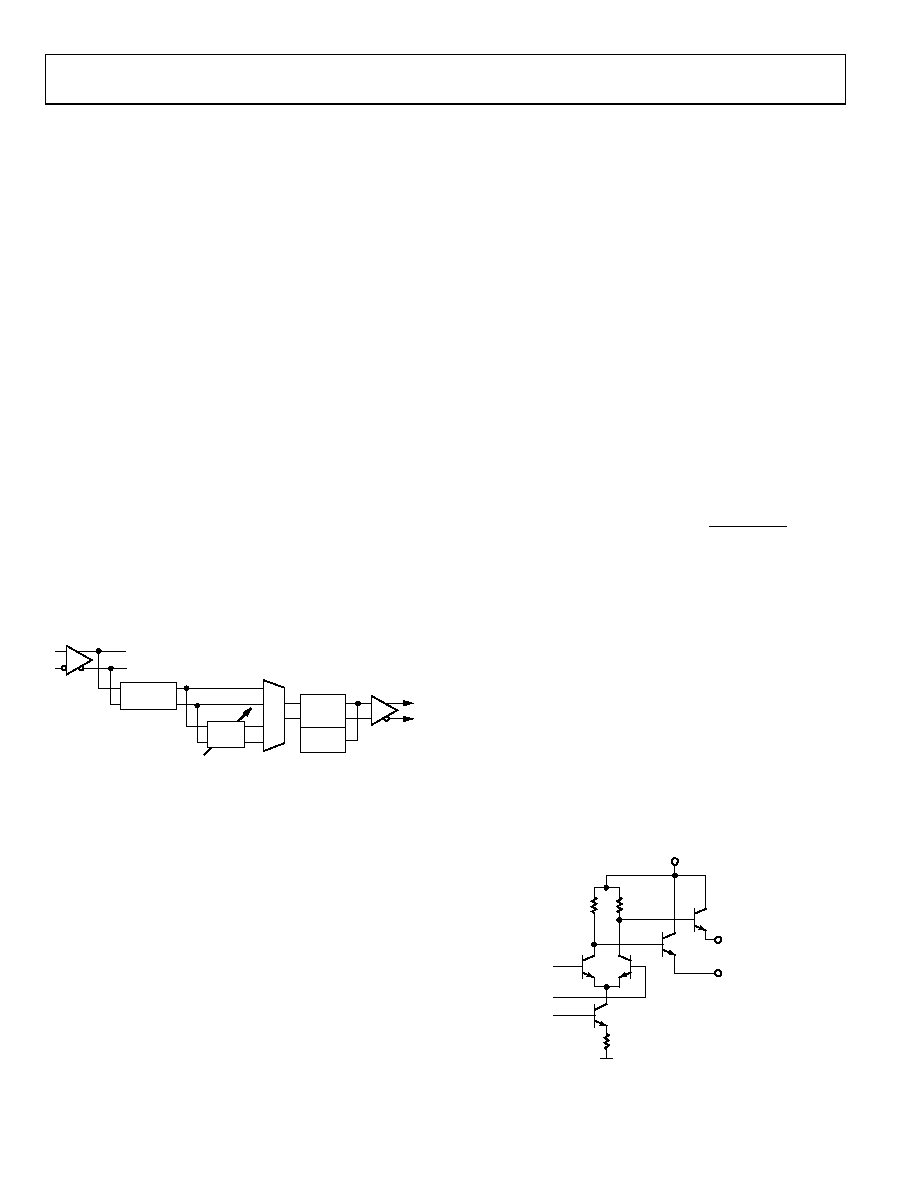
DELAY BLOCK
OUT4 (LVDS/CMOS) includes an analog delay element that
can be programmed (Register 34h to Register 36h) to give
variable time delays (ΔT) in the clock signal passing through
that output.
05287-
092
ΔT
FINE DELAY ADJUST
(32 STEPS)
FULL-SCALE: 1ns TO 10ns
OUT4 ONLY
CLOCK INPUT
÷N
SELECT
MUX
LVDS
CMOS
OUTPUT
DRIVER
Figure 26. Analog Delay (OUT4)
The amount of delay that can be used is determined by the
frequency of the clock being delayed. The amount of delay can
approach one-half cycle of the clock period. For example, for a
10 MHz clock, the delay can extend to the full 10 ns maximum
of which the delay element is capable. However, for a 100 MHz
clock (with 50% duty cycle), the maximum delay is less than
5 ns (or half of the period).
OUT4 allows a full-scale delay in the range 1 ns to 10 ns. The
full-scale delay is selected by choosing a combination of ramp
current and the number of capacitors by writing the appropriate
values into Register 35h. There are 32 fine delay settings for
each full scale, set by Register 36h.
This path adds some jitter greater than that specified for the
nondelay outputs. This means that the delay function should be
used primarily for clocking digital chips, such as FPGA, ASIC,
DUC, and DDC, rather than for data converters. The jitter is
higher for long full scales (~10 ns). This is because the delay
block uses a ramp and trip points to create the variable delay. A
longer ramp means more noise might be introduced.
Calculating the Delay
The following values and equations are used to calculate the
delay of the delay block.
Value of Ramp Current Control Bits (Register 35h or Register 39h
<2:0>) = Iramp_bits
IRAMP (μA) = 200 × (Iramp_bits + 1)
No. of Caps = No. of 0s + 1 in Ramp Control Capacitor
(Register 35h or Register 39h <5:3>), that is, 101 = 1 + 1 = 2;
110 = 2; 100 = 2 + 1 = 3; 001 = 2 + 1 = 3; 111 = 0 + 1 = 1)
Delay_Range (ns) = 200 × [(No. of Caps + 3)/(IRAMP)] × 1.3286
()
6
1
10
1600
0.34
ns
4
×
+
×
+
=
RAMP
I
Caps
of
No.
I
Offset
Delay_Full_Scale (ns) = Delay_Range + Offset
Fine_Adj = Value of Delay Fine Adjust (Register 36h or
Register 3Ah <5:1>), that is, 11111 = 31
Delay (ns) = Offset + Delay_Range × Fine_adj × (1/31)
OUTPUTS
The AD9512 offers three different output level choices:
LVPECL, LVDS, and CMOS. OUT0 to OUT2 are LVPECL only.
OUT3 and OUT4 can be selected as either LVDS or CMOS.
Each output can be enabled or turned off as needed to save
power.
The simplified equivalent circuit of the LVPECL outputs is
shown in Figure 27.
05287-
037
3.3V
OUT
OUTB
GND
Figure 27. LVPECL Output Simplified Equivalent Circuit
相关PDF资料 |
PDF描述 |
|---|---|
| X9418WV24T1 | IC XDCP DUAL 64-TAP 10K 24-TSSOP |
| ADF4351BCPZ-RL7 | IC SYNTH PLL VCO 32LFCSP |
| V24A24H300BF2 | CONVERTER MOD DC/DC 24V 300W |
| M83723/95R10057 | CONN PLUG 5POS STRAIGHT W/SCKT |
| V24A15H300BL | CONVERTER MOD DC/DC 15V 300W |
相关代理商/技术参数 |
参数描述 |
|---|---|
| AD9512-EP | 制造商:AD 制造商全称:Analog Devices 功能描述:1.2 GHz Clock Distribution IC, 1.6 GHz Inputs, Dividers, Five Outputs |
| AD9512-PCB | 制造商:AD 制造商全称:Analog Devices 功能描述:1.2 GHz Clock Distribution IC, 1.6 GHz Inputs, Dividers, Delay Adjust, Five Outputs |
| AD9512UCPZ-EP | 功能描述:IC CLOCK DIST 5OUT PLL 48LFCSP RoHS:是 类别:集成电路 (IC) >> 时钟/计时 - 时钟发生器,PLL,频率合成器 系列:- 标准包装:2,000 系列:- 类型:PLL 时钟发生器 PLL:带旁路 输入:LVCMOS,LVPECL 输出:LVCMOS 电路数:1 比率 - 输入:输出:2:11 差分 - 输入:输出:是/无 频率 - 最大:240MHz 除法器/乘法器:是/无 电源电压:3.135 V ~ 3.465 V 工作温度:0°C ~ 70°C 安装类型:表面贴装 封装/外壳:32-LQFP 供应商设备封装:32-TQFP(7x7) 包装:带卷 (TR) |
| AD9512UCPZ-EP-R7 | 功能描述:IC CLOCK DIST 5OUT PLL 48LFCSP RoHS:是 类别:集成电路 (IC) >> 时钟/计时 - 时钟发生器,PLL,频率合成器 系列:- 标准包装:2,000 系列:- 类型:PLL 时钟发生器 PLL:带旁路 输入:LVCMOS,LVPECL 输出:LVCMOS 电路数:1 比率 - 输入:输出:2:11 差分 - 输入:输出:是/无 频率 - 最大:240MHz 除法器/乘法器:是/无 电源电压:3.135 V ~ 3.465 V 工作温度:0°C ~ 70°C 安装类型:表面贴装 封装/外壳:32-LQFP 供应商设备封装:32-TQFP(7x7) 包装:带卷 (TR) |
| AD9513 | 制造商:AD 制造商全称:Analog Devices 功能描述:800 MHz Clock Distribution IC, Dividers, Delay Adjust, Three Outputs |
发布紧急采购,3分钟左右您将得到回复。