- 您现在的位置:买卖IC网 > PDF目录9088 > AD9512BCPZ-REEL7 (Analog Devices Inc)IC CLOCK DIST 5OUT PLL 48LFCSP PDF资料下载
参数资料
| 型号: | AD9512BCPZ-REEL7 |
| 厂商: | Analog Devices Inc |
| 文件页数: | 34/48页 |
| 文件大小: | 0K |
| 描述: | IC CLOCK DIST 5OUT PLL 48LFCSP |
| 标准包装: | 750 |
| 类型: | 扇出缓冲器(分配),除法器 |
| PLL: | 无 |
| 输入: | 时钟 |
| 输出: | CMOS,LVDS,LVPECL |
| 电路数: | 1 |
| 比率 - 输入:输出: | 2:5 |
| 差分 - 输入:输出: | 是/是 |
| 频率 - 最大: | 1.2GHz |
| 除法器/乘法器: | 是/无 |
| 电源电压: | 3.135 V ~ 3.465 V |
| 工作温度: | -40°C ~ 85°C |
| 安装类型: | 表面贴装 |
| 封装/外壳: | 48-VFQFN 裸露焊盘,CSP |
| 供应商设备封装: | 48-LFCSP-VQ(7x7) |
| 包装: | 带卷 (TR) |
第1页第2页第3页第4页第5页第6页第7页第8页第9页第10页第11页第12页第13页第14页第15页第16页第17页第18页第19页第20页第21页第22页第23页第24页第25页第26页第27页第28页第29页第30页第31页第32页第33页当前第34页第35页第36页第37页第38页第39页第40页第41页第42页第43页第44页第45页第46页第47页第48页
AD9512
Rev. A | Page 4 of 48
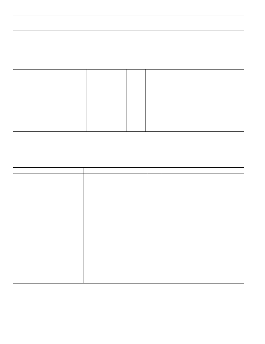
SPECIFICATIONS
Typical (Typ) is given for VS = 3.3 V ± 5%; TA = 25°C, RSET = 4.12 kΩ, unless otherwise noted. Minimum (Min) and Maximum (Max)
values are given over full VS and TA (40°C to +85°C) variation.
CLOCK INPUTS
Table 1.
Parameter
Min
Typ
Max
Unit
Test Conditions/Comments
CLOCK INPUTS (CLK1, CLK2)1
Input Frequency
0
1.6
GHz
Input Sensitivity
1502
mV p-p
Jitter performance can be improved with higher slew
rates (greater swing).
Input Level
23
V p-p
Larger swings turn on the protection diodes and can
degrade jitter performance.
Input Common-Mode Voltage, VCM
1.5
1.6
1.7
V
Self-biased; enables ac coupling.
Input Common-Mode Range, VCMR
1.3
1.8
V
With 200 mV p-p signal applied; dc-coupled.
Input Sensitivity, Single-Ended
150
mV p-p
CLK2 ac-coupled; CLK2B ac bypassed to RF ground.
Input Resistance
4.0
4.8
5.6
kΩ
Self-biased.
Input Capacitance
2
pF
1 CLK1 and CLK2 are electrically identical; each can be used as either differential or single-ended input.
2 With a 50 Ω termination, this is 12.5 dBm.
3 With a 50 Ω termination, this is +10 dBm.
CLOCK OUTPUTS
Table 2.
Parameter
Min
Typ
Max
Unit
Test Conditions/Comments
LVPECL CLOCK OUTPUTS
Termination = 50 Ω to VS 2 V
OUT0, OUT1, OUT2; Differential
Output level 3Dh (3Eh) (3Fh)<3:2> = 10b
Output Frequency
1200
MHz
See Figure 14
Output High Voltage (VOH)
VS 1.22
VS 0.98
VS 0.93
V
Output Low Voltage (VOL)
VS 2.10
VS 1.80
VS 1.67
V
Output Differential Voltage (VOD)
660
810
965
mV
LVDS CLOCK OUTPUTS
Termination = 100 Ω differential; default
OUT3, OUT4; Differential
Output level 40h (41h)<2:1> = 01b
3.5 mA termination current
Output Frequency
800
MHz
See Figure 15
Differential Output Voltage (VOD)
250
360
450
mV
Delta VOD
25
mV
Output Offset Voltage (VOS)
1.125
1.23
1.375
V
Delta VOS
25
mV
Short-Circuit Current (ISA, ISB)
14
24
mA
Output shorted to GND
CMOS CLOCK OUTPUTS
OUT3, OUT4
Single-ended measurements;
B outputs: inverted, termination open
Output Frequency
250
MHz
With 5 pF load each output; see Figure 16
Output Voltage High (VOH)
VS 0.1
V
@ 1 mA load
Output Voltage Low (VOL)
0.1
V
@ 1 mA load
相关PDF资料 |
PDF描述 |
|---|---|
| X9418WV24T1 | IC XDCP DUAL 64-TAP 10K 24-TSSOP |
| ADF4351BCPZ-RL7 | IC SYNTH PLL VCO 32LFCSP |
| V24A24H300BF2 | CONVERTER MOD DC/DC 24V 300W |
| M83723/95R10057 | CONN PLUG 5POS STRAIGHT W/SCKT |
| V24A15H300BL | CONVERTER MOD DC/DC 15V 300W |
相关代理商/技术参数 |
参数描述 |
|---|---|
| AD9512-EP | 制造商:AD 制造商全称:Analog Devices 功能描述:1.2 GHz Clock Distribution IC, 1.6 GHz Inputs, Dividers, Five Outputs |
| AD9512-PCB | 制造商:AD 制造商全称:Analog Devices 功能描述:1.2 GHz Clock Distribution IC, 1.6 GHz Inputs, Dividers, Delay Adjust, Five Outputs |
| AD9512UCPZ-EP | 功能描述:IC CLOCK DIST 5OUT PLL 48LFCSP RoHS:是 类别:集成电路 (IC) >> 时钟/计时 - 时钟发生器,PLL,频率合成器 系列:- 标准包装:2,000 系列:- 类型:PLL 时钟发生器 PLL:带旁路 输入:LVCMOS,LVPECL 输出:LVCMOS 电路数:1 比率 - 输入:输出:2:11 差分 - 输入:输出:是/无 频率 - 最大:240MHz 除法器/乘法器:是/无 电源电压:3.135 V ~ 3.465 V 工作温度:0°C ~ 70°C 安装类型:表面贴装 封装/外壳:32-LQFP 供应商设备封装:32-TQFP(7x7) 包装:带卷 (TR) |
| AD9512UCPZ-EP-R7 | 功能描述:IC CLOCK DIST 5OUT PLL 48LFCSP RoHS:是 类别:集成电路 (IC) >> 时钟/计时 - 时钟发生器,PLL,频率合成器 系列:- 标准包装:2,000 系列:- 类型:PLL 时钟发生器 PLL:带旁路 输入:LVCMOS,LVPECL 输出:LVCMOS 电路数:1 比率 - 输入:输出:2:11 差分 - 输入:输出:是/无 频率 - 最大:240MHz 除法器/乘法器:是/无 电源电压:3.135 V ~ 3.465 V 工作温度:0°C ~ 70°C 安装类型:表面贴装 封装/外壳:32-LQFP 供应商设备封装:32-TQFP(7x7) 包装:带卷 (TR) |
| AD9513 | 制造商:AD 制造商全称:Analog Devices 功能描述:800 MHz Clock Distribution IC, Dividers, Delay Adjust, Three Outputs |
发布紧急采购,3分钟左右您将得到回复。