- 您现在的位置:买卖IC网 > PDF目录9088 > AD9512BCPZ-REEL7 (Analog Devices Inc)IC CLOCK DIST 5OUT PLL 48LFCSP PDF资料下载
参数资料
| 型号: | AD9512BCPZ-REEL7 |
| 厂商: | Analog Devices Inc |
| 文件页数: | 28/48页 |
| 文件大小: | 0K |
| 描述: | IC CLOCK DIST 5OUT PLL 48LFCSP |
| 标准包装: | 750 |
| 类型: | 扇出缓冲器(分配),除法器 |
| PLL: | 无 |
| 输入: | 时钟 |
| 输出: | CMOS,LVDS,LVPECL |
| 电路数: | 1 |
| 比率 - 输入:输出: | 2:5 |
| 差分 - 输入:输出: | 是/是 |
| 频率 - 最大: | 1.2GHz |
| 除法器/乘法器: | 是/无 |
| 电源电压: | 3.135 V ~ 3.465 V |
| 工作温度: | -40°C ~ 85°C |
| 安装类型: | 表面贴装 |
| 封装/外壳: | 48-VFQFN 裸露焊盘,CSP |
| 供应商设备封装: | 48-LFCSP-VQ(7x7) |
| 包装: | 带卷 (TR) |
第1页第2页第3页第4页第5页第6页第7页第8页第9页第10页第11页第12页第13页第14页第15页第16页第17页第18页第19页第20页第21页第22页第23页第24页第25页第26页第27页当前第28页第29页第30页第31页第32页第33页第34页第35页第36页第37页第38页第39页第40页第41页第42页第43页第44页第45页第46页第47页第48页
AD9512
Rev. A | Page 34 of 48
writing to Register 5Ah<0> = 1b. This update bit is self-clearing
(it is not required to write 0 to it to clear it). Since any number
of bytes of data can be changed before issuing an update
command, the update simultaneously enables all register
changes since any previous update.
Phase offsets or divider synchronization will not become
effective until a SYNC is issued (see the Single-Chip
Synchronization section).
Read
If the instruction word is for a read operation (I15 = 1b), the
next N × 8 SCLK cycles clock out the data from the address
specified in the instruction word, where N is 1 to 4 as
determined by W1:W0. The readback data is valid on the falling
edge of SCLK.
The default mode of the AD9512 serial control port is
unidirectional mode; therefore, the requested data appears on
the SDO pin. It is possible to set the AD9512 to bidirectional
mode by writing the SDO enable register at 00h<7> = 1b. In
bidirectional mode, the readback data appears on the SDIO pin.
A readback request reads the data that is in the serial control
port buffer area, not the active data in the AD9512’s actual
control registers.
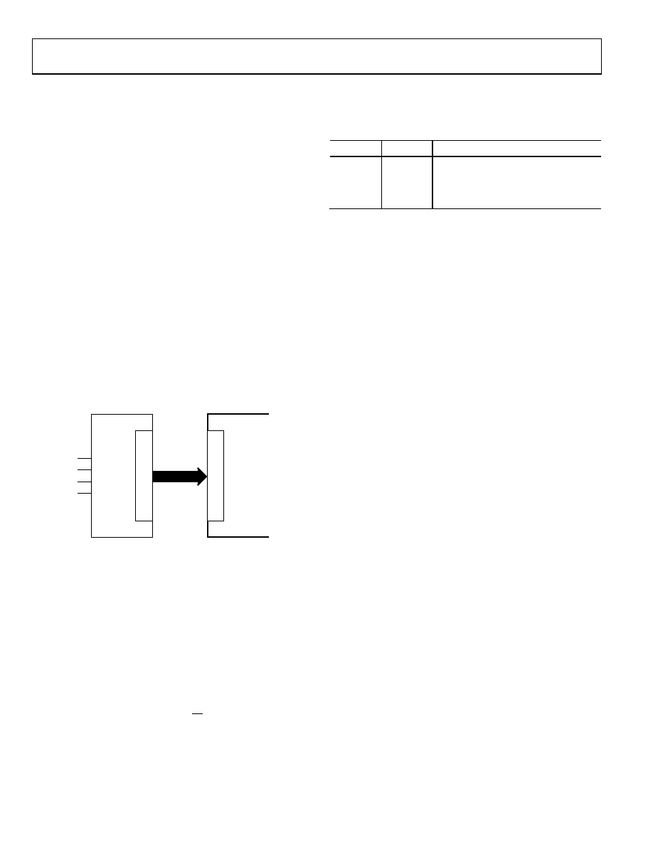
05287-
095
SCLK
SDIO
SDO
CSB
UPDATE
REGISTERS
5Ah <0>
SERIAL
CONTROL
PORT
REGISTER
BUFFERS
AD9512
CORE
CONTROL
REGISTERS
Figure 31. Relationship Between Serial Control Port Register Buffers and
Control Registers of the AD9512
The AD9512 uses Address 00h to Address 5Ah. Although the
AD9512 serial control port allows both 8-bit and 16-bit
instructions, the 8-bit instruction mode provides access to five
address bits (A4 to A0) only, which restricts its use to the
address space 00h to 01F. The AD9512 defaults to 16-bit
instruction mode on power-up. The 8-bit instruction mode
(although defined for this serial control port) is not useful for
the AD9512; therefore, it is not discussed further in this data
sheet.
THE INSTRUCTION WORD (16 BITS)
The MSB of the instruction word is R/W, which indicates
whether the instruction is a read or a write. The next two bits,
W1:W0, indicate the length of the transfer in bytes. The final 13
bits are the addresses (A12:A0) at which to begin the read or
write operation.
For a write, the instruction word is followed by the number of
bytes of data indicated by Bits W1:W0, which is interpreted
according to Table 14.
Table 14. Byte Transfer Count
W1
W0
Bytes to Transfer
0
1
0
1
2
1
0
3
1
4
A12:A0
: These 13 bits select the address within the register map
that is written to or read from during the data transfer portion
of the communications cycle. The AD9512 does not use all of
the 13-bit address space. Only Bits A6:A0 are needed to cover
the range of the 5Ah registers used by the AD9512. Bits A12:A7
must always be 0b. For multibyte transfers, this address is the
starting byte address. In MSB first mode, subsequent bytes
increment the address.
MSB/LSB FIRST TRANSFERS
The AD9512 instruction word and byte data may be MSB first
or LSB first. The default for the AD9512 is MSB first. The LSB
first mode may be set by writing 1b to Register 00h<6>. This
takes effect immediately (because it only affects the operation of
the serial control port) and does not require that an update be
executed. Immediately after the LSB first bit is set, all serial
control port operations are changed to LSB first order.
When MSB first mode is active, the instruction and data bytes
must be written from MSB to LSB. Multibyte data transfers in
MSB first format start with an instruction byte that includes the
register address of the most significant data byte. Subsequent
data bytes must follow in order from high address to low
address. In MSB first mode, the serial control port internal
address generator decrements for each data byte of the
multibyte transfer cycle.
When LSB_First = 1b (LSB first), the instruction and data bytes
must be written from LSB to MSB. Multibyte data transfers in
LSB first format start with an instruction byte that includes the
register address of the least significant data byte followed by
multiple data bytes. The serial control port internal byte address
generator increments for each byte of the multibyte transfer
cycle.
The AD9512 serial control port register address decrements
from the register address just written toward 0000h for
multibyte I/O operations if the MSB first mode is active
(default). If the LSB first mode is active, the serial control port
register address increments from the address just written
toward 1FFFh for multibyte I/O operations.
Unused addresses are not skipped during multibyte I/O
operations; therefore, it is important to avoid multibyte I/O
operations that would include these addresses.
相关PDF资料 |
PDF描述 |
|---|---|
| X9418WV24T1 | IC XDCP DUAL 64-TAP 10K 24-TSSOP |
| ADF4351BCPZ-RL7 | IC SYNTH PLL VCO 32LFCSP |
| V24A24H300BF2 | CONVERTER MOD DC/DC 24V 300W |
| M83723/95R10057 | CONN PLUG 5POS STRAIGHT W/SCKT |
| V24A15H300BL | CONVERTER MOD DC/DC 15V 300W |
相关代理商/技术参数 |
参数描述 |
|---|---|
| AD9512-EP | 制造商:AD 制造商全称:Analog Devices 功能描述:1.2 GHz Clock Distribution IC, 1.6 GHz Inputs, Dividers, Five Outputs |
| AD9512-PCB | 制造商:AD 制造商全称:Analog Devices 功能描述:1.2 GHz Clock Distribution IC, 1.6 GHz Inputs, Dividers, Delay Adjust, Five Outputs |
| AD9512UCPZ-EP | 功能描述:IC CLOCK DIST 5OUT PLL 48LFCSP RoHS:是 类别:集成电路 (IC) >> 时钟/计时 - 时钟发生器,PLL,频率合成器 系列:- 标准包装:2,000 系列:- 类型:PLL 时钟发生器 PLL:带旁路 输入:LVCMOS,LVPECL 输出:LVCMOS 电路数:1 比率 - 输入:输出:2:11 差分 - 输入:输出:是/无 频率 - 最大:240MHz 除法器/乘法器:是/无 电源电压:3.135 V ~ 3.465 V 工作温度:0°C ~ 70°C 安装类型:表面贴装 封装/外壳:32-LQFP 供应商设备封装:32-TQFP(7x7) 包装:带卷 (TR) |
| AD9512UCPZ-EP-R7 | 功能描述:IC CLOCK DIST 5OUT PLL 48LFCSP RoHS:是 类别:集成电路 (IC) >> 时钟/计时 - 时钟发生器,PLL,频率合成器 系列:- 标准包装:2,000 系列:- 类型:PLL 时钟发生器 PLL:带旁路 输入:LVCMOS,LVPECL 输出:LVCMOS 电路数:1 比率 - 输入:输出:2:11 差分 - 输入:输出:是/无 频率 - 最大:240MHz 除法器/乘法器:是/无 电源电压:3.135 V ~ 3.465 V 工作温度:0°C ~ 70°C 安装类型:表面贴装 封装/外壳:32-LQFP 供应商设备封装:32-TQFP(7x7) 包装:带卷 (TR) |
| AD9513 | 制造商:AD 制造商全称:Analog Devices 功能描述:800 MHz Clock Distribution IC, Dividers, Delay Adjust, Three Outputs |
发布紧急采购,3分钟左右您将得到回复。